


半金属Bi由于具有较强的自旋轨道耦合作用,是构成拓扑复合材料的关键化学元素[1,2]。因Bi具有较大的Fermi波长,可能引起量子尺寸效应,存在竞争性的结构相,Bi更多以薄膜的形式吸引了研究者们[3~9]的高度关注。研究者[10~12]通过实验研究发现,Bi的表面状态具有很高的金属性,这与Bi晶体的半金属性质截然不同。进一步研究[13,14]表明,随着厚度的减小,Bi(111)薄膜可以转变为半导体。Koroteev等[3]通过第一性原理计算预测一个双层(bilayer,BL)厚的Bi(111)薄膜具有半导体性质;而Liu等[15]预测1~4 BL厚的Bi(111)薄膜均为半导体性质;Wang等[16]则预测1~2 BL厚的Bi(111)薄膜为半导体性质。分析认为,不同研究者所得结论的差异除了受计算软件、参数设置的影响之外,还与所采用的Bi薄膜晶格常数有很大关系,因此考察晶格常数对能带的影响极为重要。
应变是改变晶格常数最为直接的方式,长期以来用于调节半导体的电子性能[17,18]。加之在实验制备薄膜的过程中,薄膜与衬底之间由于晶格失配引起的界面畸变不可避免。如在Bi2Se3或Bi2Te3衬底上生长Bi(111)薄膜时,薄膜面内晶格常数分别要承受10%和3.5%的压缩应变[19~21],这种应变必然会对Bi薄膜的表面导电特性产生影响。一些研究者[22~24]利用第一性原理计算,研究了对1 BL厚Bi(111)薄膜施加双轴应变后,产生的半导体向半金属的转变以及拓扑性质的变化。但是,对于应变过程中Bi(111)薄膜晶体结构以及能带结构的演变细节、趋势以及变化机制研究较少。另外,除了1 BL厚的Bi(111)薄膜之外,其他厚度的Bi(111)薄膜在应变作用下的能带变化尚未可知。
1 计算方法
本工作利用基于密度泛函理论(density functional theory,DFT)的第一性原理计算,通过VASP软件包[29]完成。原子实和价电子之间的相互作用采用投影缀加波赝势法(projector augmented wave method,PAW法)描述[30],选择广义梯度近似的Perdew-Burke-Ernzerhof (PBE)交换关联势[31]。为了避免z方向上周期性结构之间的相互作用,设置厚度为1.5 nm的真空层。平面波截断能为400 eV,晶胞Brillouin区Monkhorst-Pack k点网格为18 × 18 × 1[32]。晶胞内所有原子进行了完全弛豫,自洽计算中连续两步之间的收敛判据为10-5 eV,离子弛豫过程中作用力不超过0.10 eV/nm。自旋轨道耦合作用包含在电子自洽计算当中。
应变场通过更改晶格常数,结合几何优化过程中改变原子的自由度来施加,应变(ε)定义为:
式中,a和a0分别为应变和平衡下的晶格常数。应变范围为-10%~10%,负值表示压缩应变,正值表示拉伸应变。
2 计算结果与分析
2.1 不同厚度Bi(111)薄膜的表面特性
晶体Bi属于菱形六面体结构,也可用六角形结构直观表示,如图1a所示。每个原子具有3个等距的最近邻原子与3个等距的次近邻原子,这导致沿着垂直于(111)面方向形成典型的双层结构,以ABC方式进行堆叠。Bi(111)面属于屈曲蜂窝结构,用3个重要的结构参数:晶格常数(a)、双层内间距(d1)以及层间间距(d2)来描述,如图1b所示。初始Bi薄膜相关参数从优化后的Bi晶体结构直接获取,a = b = 0.459 nm,c = 1.211 nm,d1 = 0.160 nm,与实验值(a = b = 0.454 nm,c = 1.181 nm,d1 = 0.159 nm)[33,34]相比,符合较好。图1c给出了计算所得Bi(111)薄膜的晶格常数a随层数的变化情况以及其与实验数值[6]的对比。可以看出,随着层数增加,晶格常数不断增大,逐渐趋向于Bi晶体值,优化得到的晶格常数与实验值相比误差在2.5%以内,表明当前的方法和参数设置合理,为能够准确、可靠地研究薄膜的半导体-半金属转变打下基础。图1d给出了d1和d2随层数变化的曲线。发现随着层数的增加,层内间距和层间间距均呈下降趋势,面内晶格常数增大,面间间距减小,体现了Poisson效应。
图1
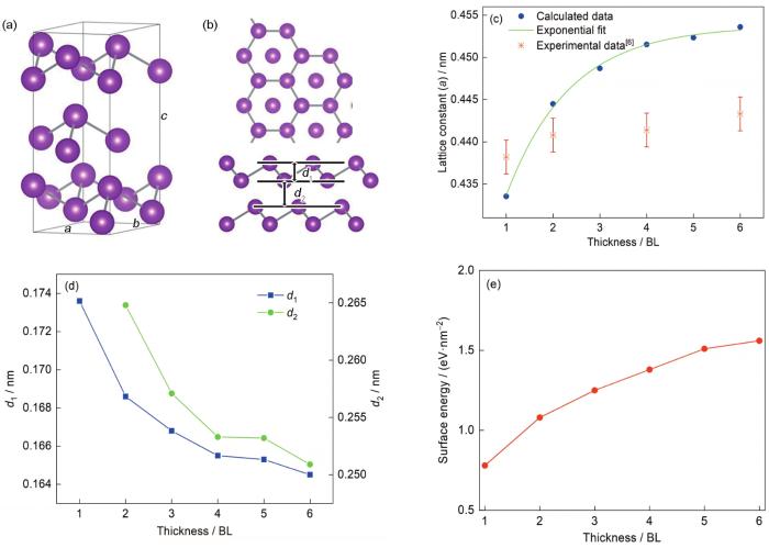
图1
Bi晶体结构、薄膜结构示意图以及薄膜性质随厚度的变化
Fig.1
Hexagonal crystal structure (a, b, and c are lattice constants, a = b) (a), top and side views of 2 bilayers (BLs) atomic structure together (b), the optimized surface unit cell parameter as a function of the number of Bi BLs and experimental data[6] (c), the variation of intra-BL (d1) and inter-BL (d2) distances, as a function of the number of BLs (d), and calculated surface energy for free-standing Bi(111) films as a function of the number of BLs (e)
为了评价Bi薄膜表面构型的稳定性,研究了不同厚度下Bi(111)面的表面能。表面能指体相材料形成表面所需的能量,通常表面能越小,表面越易形成,稳定性越强,具体计算方式如下[35]:
式中,Esurf为表面能,Eslab为薄膜总能量,n为薄膜的总原子数,Ebulk为Bi晶体中单原子能量,A为薄膜表面积。Bi(111)面的表面能计算结果如图1e所示。可以看出,随着层数的增加,表面能增大并逐渐趋向于稳定值(1.60 eV/nm2),在1 BL厚时,表面能最小,具有较高的表面稳定性。
为了详细探讨Bi(111)薄膜的电学性质,基于上述优化后的结构,利用第一性原理计算了1~5 BL厚的Bi(111)薄膜的能带结构,结果如图2所示。1 BL厚时,导带底(conduction band minimum,CBM)在高对称点Γ (0, 0, 0)处,而价带顶(valence band maximum,VBM)由于Rashba型分裂,其位置相对于Γ点有所偏移,形成带隙为0.474 eV的间接带隙半导体,这不同于Bi晶体的半金属性质,表明1 BL厚薄膜顶面与底面强烈的耦合作用(图2a)。对2 BL厚的Bi(111)薄膜,由于层间相互作用的影响,带隙减小到0.051 eV,仍呈现间接带隙半导体特征(图2b)。而当Bi(111)薄膜厚度为3 BL和4 BL时,导带底和价带顶接触Fermi能级,呈现半金属特性(图2c和d)。当厚度为5 BL时,部分能带越过Fermi能级,呈现金属特性(图2e)。图2f绘制了直接带隙和间接带隙随薄膜厚度的变化曲线。可以看出直接带隙一直为正值,而间接带隙在3 BL厚时,变为负值,由半导体性质变为半金属性质。
图2
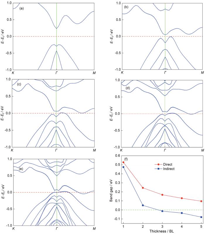
图2
1~5 BL厚Bi(111)薄膜的能带结构及带隙
Fig.2
Band structures of 1-5 BL thickness Bi(111) film (a-e), direct and indirect energy band gap curves as a function of the film thickness (f) (E—energy, Ef—Fermi energy)
通过对不同厚度Bi(111)薄膜能带结构的研究,发现其几何结构和电子性质具有厚度依赖性。随着厚度增加,晶格常数增大,屈曲高度降低,表面能增加,带隙不断减小,在3 BL厚时,Bi薄膜将发生半导体向半金属的转变。
2.2 应变对1 BL Bi(111)薄膜结构与电学性能的影响
2.2.1 应变引发的能量、结构变化
施加应变后1 BL厚薄膜的总能量变化示于图3a。可以看出,未施加应变时能量最低。随应变增加,能量随之升高,能量与应变近似成抛物线关系。在较小应变范围内(-2%~2%),能量变化较小;较大应变时,压缩应变的能量大于拉伸应变的能量,表明压缩应变更容易破坏薄膜的稳定性。施加应变后1 BL厚薄膜屈曲高度与键长随应变的变化示于图3b。屈曲高度百分比变化与应变近似成相反数的关系。如2%的拉伸应变导致屈曲高度减小1.96%,4%的压缩应变导致屈曲高度增大4.13%,这与Poisson效应有关,平面内的双轴应变促使原子在垂直平面方向上进行弛豫,从而改变了屈曲高度。Poisson效应的这种作用使得键长稳定在平衡值附近,尽量维持薄膜的稳定结构,如最大10%的拉伸应变对应键长最大百分比变化为4.06%。另外,当压缩应变大于6%时,屈曲高度迅速增加,键长也由原先的下降趋势,变为上升,图3a相应的薄膜能量也快速增加,这可能与较大的压缩应变加大了原子之间的排斥作用有关。
图3
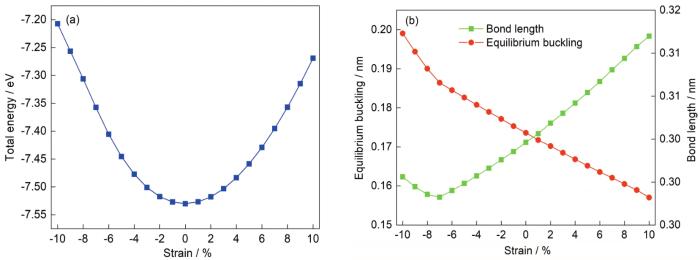
图3
施加双轴应变时1 BL厚Bi(111)薄膜能量和结构的变化
Fig.3
Variations of total energy (a), bond length and equilibrium buckling (b) of 1 BL thickness Bi(111) film with different strains
2.2.2 应变引发的能带结构变化
图4
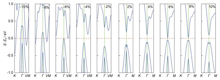
图4
1 BL厚Bi(111)薄膜在不同应变下的能带结构
Fig.4
Electronic band structures of 1 BL thickness Bi(111) film with different strains
图5
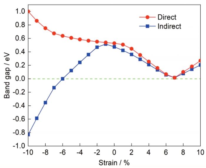
图5
1 BL厚Bi(111)薄膜直接带隙和间接带隙随应变的变化
Fig.5
Variations of direct and indirect energy band gaps of 1 BL thickness Bi(111) film with different strains
在压缩应变过程中,随着应变的增加,带隙先增大,在-1%应变时达到最大值0.523 eV;其后带隙逐渐减小,在-6%时,导带底能量与价带顶能量恰好相等,带隙为0;超过-6%应变后,带隙变为负值,由原先的半导体性质转变为半金属、金属特性;另外,-2%应变时导带底位置由Γ点转移到V (0, 0.298, 0)处,-4%应变时能带分裂消失,价带顶被Γ点占据,由于价带顶与导带底位置的不同,1 BL厚Bi(111)薄膜在压缩应变下并未发现间接到直接带隙的转变。
当薄膜受拉伸形变时,随应变的增加,导带底的位置并未发生变化,而价带顶由于能带分裂不断减弱,逐渐向Γ点靠近。结合带隙图分析,随应变的增加,直接带隙、间接带隙先减小后增大,在7%左右达到最小值,此时直接带隙、间接带隙相等。进一步针对7%应变附近的拉伸研究表明,在6.4%~7.0%应变之间,能带分裂消失,薄膜由间接带隙转变为直接带隙,在6.4%应变时直接带隙最大为0.034 eV,6.8%应变时带隙为0。因此,基于该结果可知,拉伸应变可以诱发1 BL厚 Bi(111)薄膜间接-直接-间接带隙的转变。
2.2.3 应变对Bi薄膜电子结构的调控机制
为了进一步揭示带隙变化以及半导体到半金属特性的转变根源,本工作给出了导带底能量(energy for the conduction band minimum (CBM),ECBM)和价带顶能量(energy for the valence band maximum (VBM),EVBM)随应变的变化情况,结果如图6a所示,带隙定义为2者能量的差值。可以看出,拉伸应变下,随应变量的增加,1 BL厚Bi(111)薄膜的ECBM和EVBM呈现下降趋势,但ECBM的下降速率大于EVBM,从而导致2者之间的差值不断减小,到7%应变时达到最小,对应于图5中拉伸应变条件下带隙减小的阶段。随后2者变化趋势发生了转折(交换),例如EVBM超过7%应变后的下降趋势与ECBM在7%应变前的变化趋势相似。这种能量的特殊变化,以及6.8%应变时的0带隙现象,推测与应变诱发能带反转有关。为了验证这种猜测,进一步计算了4%和8%应变下价带在Γ点 (valence band at Γ,VB-Γ)和导带在Γ点(conduction band at Γ,CB-Γ)的局域电荷密度,其等值面取10.12 e/nm3,结果如图6b所示。可以看出,8%应变下VB-Γ处的局域电荷密度与4%应变下CB-Γ处的局域电荷密度相同;而8%应变下CB-Γ处的局域电荷密度与4%应变下VB-Γ处的局域电荷密度有所差异,但考虑a和b轴的等价性,2者之间可以通过一定的对称操作互相转换,即2者能量对双轴应变的响应是一致的。
图6

图6
1 BL厚Bi(111)薄膜导带底能量(ECBM)和价带顶能量(EVBM)随应变的变化及局域电荷密度分布
Fig.6
Variations of ECBM and EVBM as a function of strain (a), and local charge density at CB-Γ and VB-Γ (strain ε = 4% and 8%) (b) of 1 BL thickness Bi(111) film (CBM—conduction band minimum, VBM—valence band maximum, ECBM—energy for the CBM, EVBM—energy for the VBM, CB-Γ—conduction band at Γ, VB-Γ—valence band at Γ)
压缩应变下,随应变的增加,ECBM和EVBM呈现上升趋势。初始时,由于ECBM的上升速率大于EVBM,从而导致了带隙增加,在-1%时达到了带隙最大值;随后ECBM变化趋势发生转折,上升速率显著减慢,开始小于EVBM的上升速率,2者之间的差值不断减小,-6%应变时,2者能量相等;继续增大应变,EVBM大于ECBM,带隙变为负值,发生了半导体-半金属转变。结合图4的分析,ECBM变化趋势发生转折与导带底的转移相关联。为了进一步研究导带底的转移情况,绘制了导带边缘态在Γ点的能量(ECB-Γ )、V点的能量(ECB-V )随应变(-6%到6%)变化曲线,结果如图7a所示。可以看出,ECB-V 与ECB-Γ 2种能量与应变近似成线性关系:随拉伸应变的增加而减小,随压缩应变的增加而增加,且ECB-Γ 的变化率大于ECB-V。2种能量的竞争关系决定了导带底的位置:当应变小于-1%时,ECB-V 小于ECB-Γ,此时导带底位于V点,而当应变大于等于-1%时,ECB-V 大于ECB-Γ,此时导带底位于Γ点。
图7
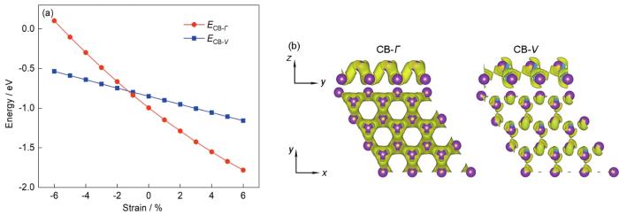
图7
1 BL厚Bi(111)薄膜导带边缘态在Γ点能量(ECB-Γ )和在V点能量(ECB-V )随应变变化以及CB-Γ、CB-V处的局域电荷密度分布
Fig.7
Variations of ECB-Γ and ECB-V as a function of strain (a), and local charge density at CB-Γ and CB-V (b) of 1 BL thickness Bi(111) film (CB-Γ—conduction band at Γ,
式中,E0为孤立原子的能量;e为元电荷,1e = 1 × 10-19 C;R为原子核间距;K为电子-电子和电子-离子之间的经典Coulomb能;S为不同原子位之间轨道的重叠积分,通常远小于1,S2更小。因此,交换积分项H在决定成键能和反键能随应变变化的行为中起主导作用,H由
在CB-V处,原子间呈反键性质,由
上述研究揭示了不同应变下导带底位置的转移机理。正是这种转变导致了1 BL厚薄膜的半导体到半金属的转变。这种现象在GaAs纳米线的研究中也被观察到[25]。
2.2.4 应变对电子、空穴有效质量的影响
为了探究应变情况下载流子输运能力的变化,根据
式中,ħ、E和k分别为约化Planck常数、电子能量和电子波数矢量,m*可以用来描述载流子输运能力的强弱。
结果表明,在无应变时,电子的有效质量为0.191me (电子质量me = 9.10956 × 10⁻³¹ kg),空穴的有效质量为0.305me,应变下电子和空穴有效质量变化情况示于图8。电子、空穴有效质量变化趋势与半导体-半金属转变、直接-间接带隙转变以及能带反转现象相对应,可结合
图8
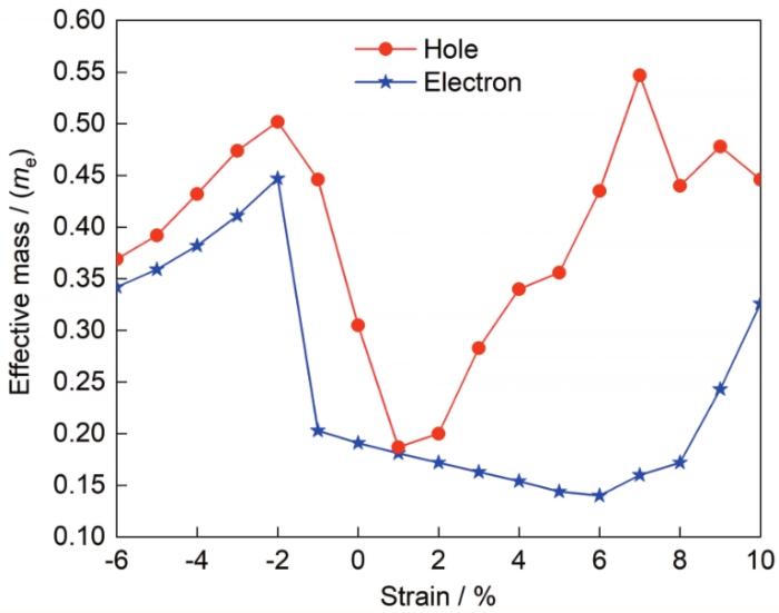
图8
1 BL厚Bi(111)薄膜中电子有效质量与空穴有效质量随应变变化曲线
Fig.8
Variations of effective masses of the electron and hole as a function of strain of 1 BL thickness Bi(111) film (me—electronic quality)
压缩应变时,导带底位置在-2%应变时开始发生偏移,电子的有效质量也随应变的增加先增加,在-2%应变时发生跳跃,达到最大值(0.447me)。随着应变的增加,在-6%应变时Bi薄膜由半导体转变为半金属,相应地电子的有效质量减小。拉伸应变时,在6%应变发生了间接-直接带隙转变以及能带反转现象,相应地电子的有效质量随应变的增加先减小后增大,在6%应变达到最小值(0.140me),这预示了在此应变下电子传输性能增强。
对于空穴的有效质量,在压缩应变时,与电子有效质量变化情况相似,随应变的增加先增加后减小;在拉伸应变时,其大小随应变的增加呈现先减小后增大最后减小的趋势,在1%应变时达到最小值(0.187me),在7%应变时达到最大值(0.547me),空穴传输相对受阻,此时能带分裂消失,能带色散减弱,继而发生了直接-间接带隙转变以及能带反转现象。
应变必然诱发能带结构的变化,从而影响电子、空穴有效质量的变化。在整个应变过程中,注意到电子的有效质量始终小于电子本身质量并且小于空穴的有效质量,表明1 BL厚Bi(111)薄膜具有较高的载流子传输能力,更加倾向于电子载流子输运。
2.3 应变对2~5 BL厚Bi(111)薄膜能带结构的影响
在Bi(111)薄膜的研究中,关于2~5 BL厚薄膜在应变下的能带变化研究较少。本工作针对2~5 BL厚的Bi(111)薄膜施加应变,计算了带隙随应变的变化情况。
图9a和b分别为2 BL厚Bi(111)薄膜在-2%~10%应变范围内的能带和带隙随应变的变化。可以看出,压缩应变下,带隙随应变的增加逐渐减小。-1%应变时带隙为0,-2%应变时带隙为负值,薄膜呈半金属特性。若继续加大应变,带隙始终为负值,呈现金属特性。2 BL厚Bi(111)薄膜压缩应变时的能带结构变化与1 BL相似,压缩应变导致导带底的转移,由原先的Γ点转移到U (0, 0.316, 0)处。导致ECB-U 小于ECB-Γ,发生导带底的转移,使得导带与价带有所重叠,薄膜由半导体特性转变为半金属特性。
图9
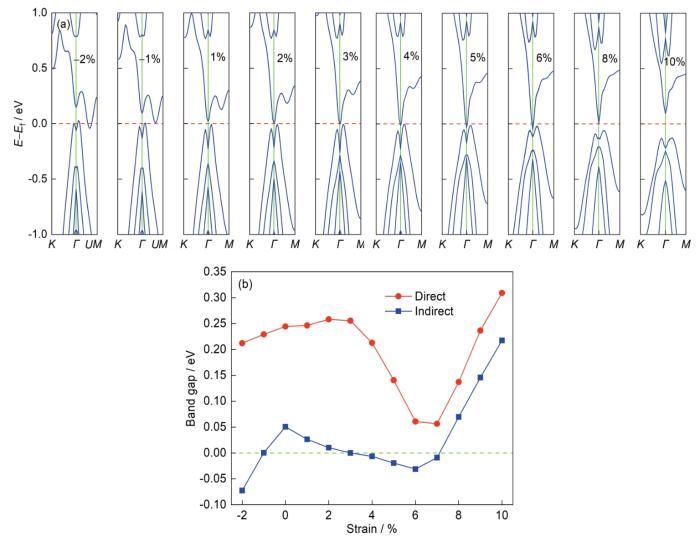
图9
2 BL厚Bi(111)薄膜能带结构及带隙随应变的变化
Fig.9
Variations of electronic band structures (a) and direct/indirect energy band gaps (b) change as a function of the strain for 2 BL thickness Bi(111) film
对于拉伸应变,随着应变的增加,带隙先减小,在3%应变时带隙为0,4%~7%应变时为半金属。通过能带图分析,在6%拉伸应变范围内,价带顶的能量约等于Fermi能,而导带底的能量相对于Fermi能不断减小,这种变化主要来源于拉伸应变导致的成键能减小,从而发生了半导体半金属的转变。施加更大的应变(8%)时转变为半导体,并且带隙随应变的增加而增加,在10%应变时可以达到0.220 eV。
拉伸应变下3~5 BL厚Bi(111)薄膜带隙变化情况如图10所示。可以看出,3者在变化趋势上具有相似之处,未应变状态时薄膜为半金属,而只需1%的拉伸应变,则会由原先的负带隙变为正带隙,带隙值随层数增加而递减。当应变大于3%时,带隙再次减小为负值,变为半金属。施加更大的应变,薄膜又变为半导体,并且可以获得较大的带隙。3 BL厚Bi薄膜在10%应变时达到最大带隙0.174 eV,4 BL厚Bi薄膜在9%应变时达到最大带隙0.101 eV,5 BL厚Bi薄膜在7%应变时达到最大带隙0.068 eV。因此,对于原先为半金属性质的3~5 BL厚Bi薄膜,施加一定的拉伸应变能够转变为半导体性质,为实验应用研究提供一定的参考。
图10

图10
3~5 BL厚Bi(111)薄膜带隙随应变的变化
Fig.10
Variations of energy band gap as a function strain for the Bi(111) films with thickness of 3 BL, 4 BL, and 5 BL
3 结论
(1) Bi(111)薄膜的晶体结构与电子结构具有厚度依赖性,随着厚度的增加,晶格常数增大,屈曲高度降低,表面能增加,带隙减小;在3 BL厚时,Bi薄膜由原先的半导体性质转变为半金属。
(2) 1 BL厚Bi(111)薄膜在拉伸应变下随应变增加带隙先减小后增加,6.8%应变时带隙为0,在此附近发生了间接-直接带隙转变以及能带反转现象;压缩应变下随应变增加带隙先增加后减小,-6%应变时发生半导体-半金属转变,通过近带电子轨道的成键性质分析,揭示了成键态、反键态对应变的不同响应速率,导致了导带底的转移,从而导致了半导体到半金属转变;应变可以有效地调节载流子输运能力,在整个应变过程中,电子的有效质量始终小于空穴的有效质量,1 BL厚Bi薄膜倾向于电子载流子输运。
(3) 对于2 BL厚Bi薄膜,较小的压缩应变(-1%)或者较小的拉伸应变(3%)都将导致半导体-半金属转变,压缩应变下的半导体-半金属转变与导带底的转移有关,这与1 BL相似。对于原先为负带隙的3~5 BL厚Bi薄膜,仅施加1%的拉伸应变可以获得正带隙,施加更大的拉伸应变可以获得较大带隙的半导体。
参考文献
Topological insulators and superconductors
[J].
Colloquium: Topological insulators
[J].
First-principles investigation of structural and electronic properties of ultrathin Bi films
[J].
Effect of thickness on the surface and electronic properties of Bi film
[J].
厚度对Bi薄膜表面特性和电学性质的影响
[J].
基于第一性原理计算方法研究了厚度对(00l)和(012)取向Bi薄膜稳定性、相变及导电性的影响。计算结果表明,随着厚度的增加,(00l)取向Bi薄膜稳定性增强,且薄膜偶数层稳定性优于奇数层;(012)取向Bi薄膜稳定性随着厚度的增加而降低,且在层数为4时,表面能与偶数层(00Ɩ)取向的薄膜相当,预示二者在该厚度时较易发生相变,分析认为与薄膜加厚过程中表面态的影响有关。随着厚度的增加,(00Ɩ)和(012)取向的Bi薄膜表现出从半导体转变为金属的特性。
Investigation of growth characteristics and semimetal-semiconductor transition of polycrystalline bismuth thin films
[J].The preferred orientation growth characteristics and surface roughness of polycrystalline bis-muth (Bi) thin films fabricated on glass substrates using the molecular beam epitaxy method were investigated at temperatures ranging from 18 to 150°C. The crystallization and morphology were analyzed in detail and the polycrystalline metal film structure-zone model (SZM) was modified to fit the polycrystalline Bi thin film. The boundary temperature between Zone T and Zone II in the SZM shifted to higher temperatures with the increase in film thickness or the decrease of growth rate. Furthermore, the effect of the thickness and surface roughness on the transport properties was investigated, especially for Bi thin films in Zone II. A two-transport channels model was adopted to reveal the influence of the film thickness on the competition between the metallic surface states and the semiconducting bulk states, which is consistent with the results of Bi single-crystal films. Therefore, the polycrystalline Bi thin films are expected to replace the single-crystal films in the application of spintronic devices.© Nan Wang et al. 2020.
Topologically nontrivial bismuth(111) thin films
[J].
Origin of flat morphology and high crystallinity of ultrathin bismuth films
[J].
Epitaxial growth of Bi thin films on Ge(111)
[J].
Electronic structure of a bismuth bilayer
[J].
Role of spin-orbit coupling and hybridization effects in the electronic structure of ultrathin Bi films
[J].
Tunable spin polarization in bismuth ultrathin film on Si(111)
[J].We performed a spin- and angle-resolved photoemission spectroscopy of bismuth ultrathin film on Si(111) with various film thickness d. We found that the spin polarization of spin-split Rashba surface states near the Brillouin-zone boundary, which is high (0.7) at d = 40 BL (bilayers), is gradually reduced on decreasing d and almost vanishes at d = 8 BL. This finding provides a novel method to generate spin-polarized electrons with tunable spin-polarization.© 2012 American Chemical Society
Fermi surface of Bi(111) measured by photoemission spectroscopy
[J].
Bi(111) thin film with insulating interior but metallic surfaces
[J].
Semimetal-to-semiconductor transition in bismuth thin films
[J].
Stable nontrivial Z2 topology in ultrathin Bi (111) films: A first-principles study
[J].
Electronic structures and topological properties of Bi(111) ultrathin films
[J].
Bending and buckling of carbon nanotubes under large strain
[J].
Strain effects on work functions of pristine and potassium-decorated carbon nanotubes
[J].
Atomic and electronic structure of ultrathin Bi(111) films grown on Bi2Te3(111) substrates: Eevidence for a strain-induced topological phase transition
[J].
Creation of helical Dirac fermions by interfacing two gapped systems of ordinary fermions
[J].Topological insulators are a unique class of materials characterized by a Dirac cone state of helical Dirac fermions in the middle of a bulk gap. When the thickness of a three-dimensional topological insulator is reduced, however, the interaction between opposing surface states opens a gap that removes the helical Dirac cone, converting the material back to a normal system of ordinary fermions. Here we demonstrate, using density function theory calculations and experiments, that it is possible to create helical Dirac fermion state by interfacing two gapped films-a single bilayer Bi grown on a single quintuple layer Bi2Se3 or Bi2Te3. These extrinsic helical Dirac fermions emerge in predominantly Bi bilayer states, which are created by a giant Rashba effect with a coupling constant of similar to 4eV. angstrom due to interfacial charge transfer. Our results suggest that this approach is a promising means to engineer topological insulator states on non-metallic surfaces.
Quasiparticle dynamics in reshaped helical Dirac cone of topological insulators
[J].
Robustness of two-dimensional topological insulator states in bilayer bismuth against strain and electrical field
[J].
Strain driven topological phase transitions in atomically thin films of group IV and V elements in the honeycomb structures
[J].
Topological phase stability and transformation of bismuthene
[J].
Origination of the direct-indirect band gap transition in strained wurtzite and zinc-blende GaAs nanowires: A first principles study
[J].
Engineering direct-indirect band gap transition in wurtzite GaAs nanowires through size and uniaxial strain
[J].
Strain modulated band gap of edge passivated armchair graphene nanoribbons
[J].
Strain-engineered direct-indirect band gap transition and its mechanism in two-dimensional phosphorene
[J].
Efficiency of ab-initio total energy calculations for metals and semiconductors using a plane-wave basis set
[J].
From ultrasoft pseudopotentials to the projector augmented-wave method
[J].
Generalized gradient approximation made simple
[J].
Special points for Brillouin-zone integrations
[J].
Nanofilm allotrope and phase transformation of ultrathin Bi film on Si(111)-7 × 7
[J].
Structure of the (111) surface of bismuth: LEED analysis and first-principles calculations
[J].
