应变工程中Bi(111)薄膜的半导体-半金属转变及其机理
Strain-Engineered Semiconductor to Semimetallic Transition and Its Mechanism in Bi(111) Film
应变工程中Bi(111)薄膜的半导体-半金属转变及其机理 |
| 任师浩, 刘永利, 孟凡顺, 祁阳 |
|
Strain-Engineered Semiconductor to Semimetallic Transition and Its Mechanism in Bi(111) Film |
| REN Shihao, LIU Yongli, MENG Fanshun, QI Yang |
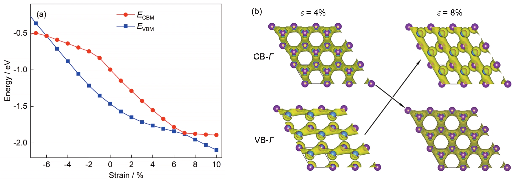
| 图6 1 BL厚Bi(111)薄膜导带底能量(ECBM)和价带顶能量(EVBM)随应变的变化及局域电荷密度分布 |
| Fig.6 Variations of ECBM and EVBM as a function of strain (a), and local charge density at CB-Γ and VB-Γ (strain ε = 4% and 8%) (b) of 1 BL thickness Bi(111) film (CBM—conduction band minimum, VBM—valence band maximum, ECBM—energy for the CBM, EVBM—energy for the VBM, CB-Γ—conduction band at Γ, VB-Γ—valence band at Γ) |
|
|