应变工程中Bi(111)薄膜的半导体-半金属转变及其机理
Strain-Engineered Semiconductor to Semimetallic Transition and Its Mechanism in Bi(111) Film
应变工程中Bi(111)薄膜的半导体-半金属转变及其机理 |
| 任师浩, 刘永利, 孟凡顺, 祁阳 |
|
Strain-Engineered Semiconductor to Semimetallic Transition and Its Mechanism in Bi(111) Film |
| REN Shihao, LIU Yongli, MENG Fanshun, QI Yang |
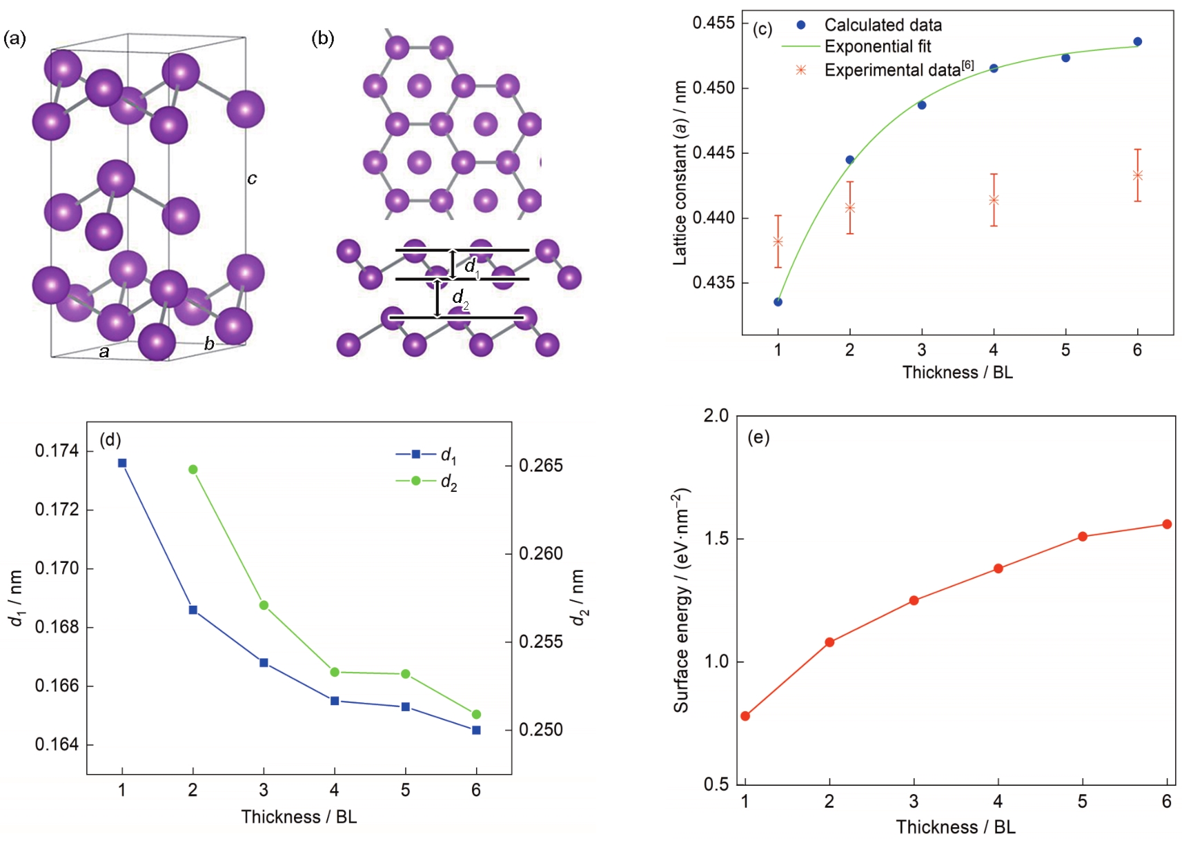
| 图1 Bi晶体结构、薄膜结构示意图以及薄膜性质随厚度的变化 |
| Fig.1 Hexagonal crystal structure (a, b, and c are lattice constants, a = b) (a), top and side views of 2 bilayers (BLs) atomic structure together (b), the optimized surface unit cell parameter as a function of the number of Bi BLs and experimental data[ |
|
|