应变工程中Bi(111)薄膜的半导体-半金属转变及其机理
Strain-Engineered Semiconductor to Semimetallic Transition and Its Mechanism in Bi(111) Film
应变工程中Bi(111)薄膜的半导体-半金属转变及其机理 |
| 任师浩, 刘永利, 孟凡顺, 祁阳 |
|
Strain-Engineered Semiconductor to Semimetallic Transition and Its Mechanism in Bi(111) Film |
| REN Shihao, LIU Yongli, MENG Fanshun, QI Yang |
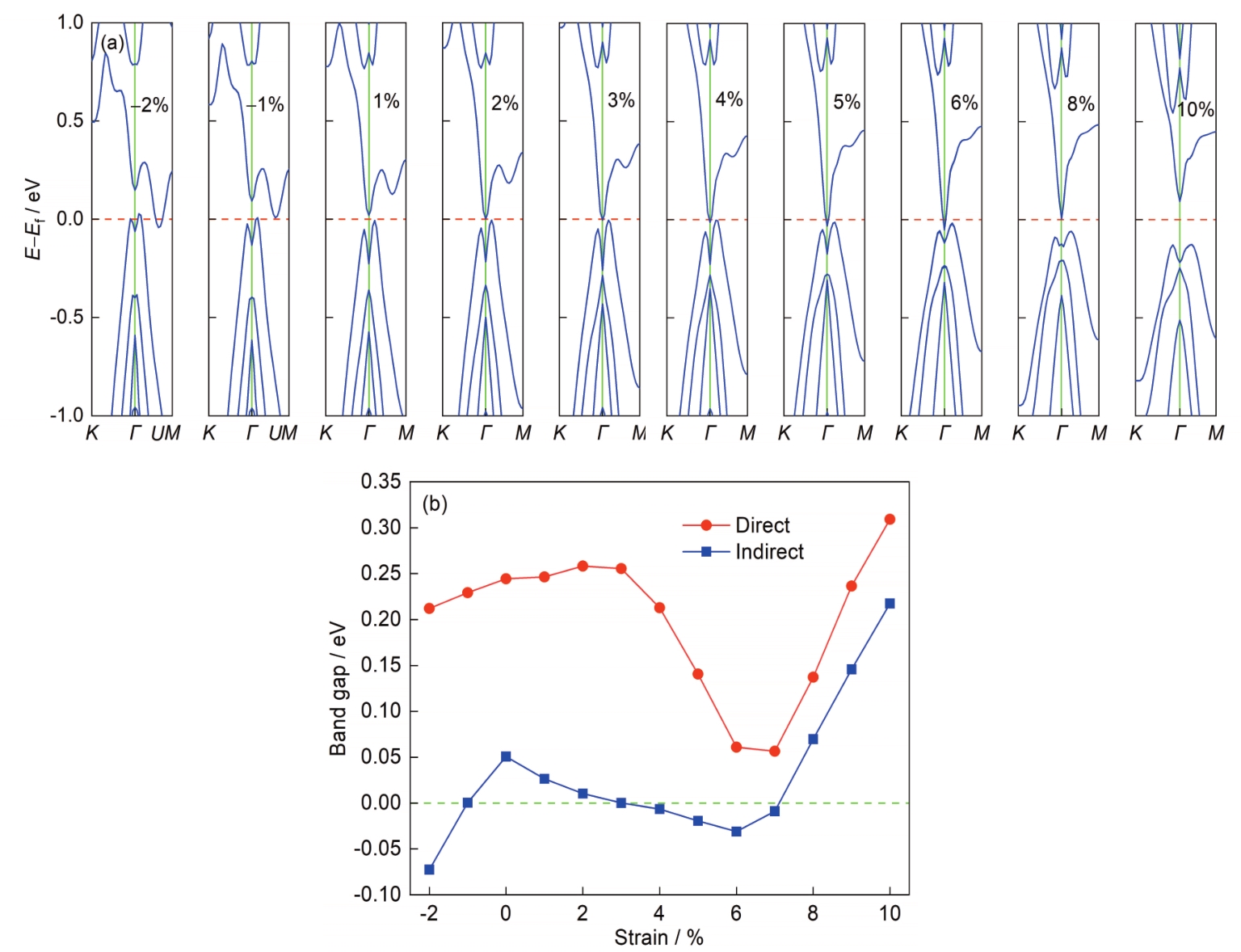
| 图9 2 BL厚Bi(111)薄膜能带结构及带隙随应变的变化 |
| Fig.9 Variations of electronic band structures (a) and direct/indirect energy band gaps (b) change as a function of the strain for 2 BL thickness Bi(111) film |
|
|