


微电子技术包括两大关键技术:芯片技术与封装技术。目前,由于引领芯片技术发展的“摩尔定律”正面临着接近自身物理极限的严峻挑战,在封装技术层次上通过系统封装与集成来实现“超越摩尔”成为微电子技术的发展方向和重大需求,推动封装技术向微型化和高性能化方向发展。微型化发展趋势下,芯片互连焊点的尺寸逐渐减小:球栅阵列(ball grid array,BGA)焊球的直径从早期的760 μm持续减小至250 μm,可控塌陷芯片连接(controlled collapse chip connection,C4)焊点直径持续减小至仅80~100 μm,再至直径仅十几微米的铜柱凸点(Cu pillar bump)。微型化发展趋势下,焊点直径每减小1个数量级,通过焊点的电流密度增加2个数量级;同时,高性能化发展趋势下,单个互连焊点所承载的功率密度显著提高。因此,先进封装技术中芯片互连焊点的电迁移(electromigration,EM)可靠性受到严峻挑战。
1861年,Gerardin[1]发现在通电后的液态Sn-Pb合金中发生Pb元素的偏聚,这是研究人员首次发现电迁移现象。电迁移现象在固态金属中的发生概率低于液态金属,因此长期未引起科研人员的重视。随着集成电路集成度不断增加,互连导线和互连焊点的尺寸持续减小,通过焊点的电流密度随直径减小呈平方增加,电迁移可靠性问题凸显。1967年,Blech和Meieran[2]发现电迁移导致Al薄膜互连导线阴极出现空洞、阳极出现凸起,这些缺陷会严重影响集成电路的可靠性。1995年,Clement和Thompson[3]发现电迁移导致Cu薄膜互连导线开路失效;1998年,Brandenburg和Yeh[4]报道了Sn-Pb共晶倒装焊点的电迁移失效行为。上述研究引起研究者对互连导线与互连焊点电迁移可靠性的重视。
1999年,国际半导体技术发展路线图(ITRS)将电迁移列为影响封装互连可靠性问题的重要因素;2003年,ITRS再次强调电迁移对高密度封装技术发展的限制;2011年,ITRS预测未来微凸点(micro-bump)的最小间距将降低至10 μm,硅通孔(through silicon via,TSV)转接板中的凸点直径仅为0.8~1.5 μm,通过微焊点的电流密度将高达104~106 A/cm2。随着电子封装技术的快速发展,由于微焊点的尺寸持续减小至微米尺度,微焊点内部微观组织缺陷和不均匀性对电迁移可靠性的影响更加显著。同时,相较于Al、Cu等互连导线,目前常用的锡基钎料合金焊点具有低熔点、微尺度、多材料、多界面以及材料间交互作用等特征,其电迁移行为更加复杂多变和难以预测,成为先进封装技术中的一个薄弱环节。因此,电迁移已成为先进封装技术中微焊点可靠性的关键问题之一。
1 电迁移研究概述
1.1 电迁移的物理本质和主要影响因素
1.1.1 电迁移的物理本质
电迁移是一种在电场作用下金属原子的定向迁移现象,其物理本质涉及电场和自由电子对金属原子的复合作用。电迁移过程中金属原子受到2种作用力的影响:① 外加电场所施加的静电场力(electrostatic force, Fel):外加电场改变了电子的量子态能级分布,使得电子的波函数在电场方向上发生偏移。这种偏移导致电子云的非对称极化,进而产生静电场力;静电场力的方向与电场方向相反,驱动金属原子向阴极方向迁移。② 电子与金属原子相互作用而产生的电子风力(electron wind force, Fwd):电流通过导体时运动的自由电子与金属原子相互作用,Fermi面附近的高能电子与金属原子核之间发生非弹性散射产生动量交换,驱动金属原子定向迁移,其本质上是量子化的动量交换,动量传递速率决定了电子风力的大小。 Fel和 Fwd的合力( F )决定了金属原子的迁移方向[5]:
式中,e为电子电荷;Zel为原子的价电荷数;Zwd为假定电子风力引起的电荷数; E 为外加电场(电场强度E = ρj,其中,ρ为电阻率,j为电流密度);Z*为有效电荷数,可以表示为:
式中,Z为金属原子的名义价态,Δ
Tammaro[6]进一步从能量的角度出发,揭示了原子在电场作用下的能量变化。在电场作用下原子会受到电子风力的作用而发生定向迁移,进而改变其在晶格中扩散所需要克服的能量势垒。这使得在电迁移过程中原子更容易顺着电子风方向扩散,因为能量势垒的变化使得原子在逆电子风方向的阻碍更大,而在顺电子风方向的阻碍更小。
1.1.2 电迁移可靠性的主要影响因素
因此,金属原子总的扩散通量(
即:
式中,C为原子浓度,D为原子扩散系数,
即当电迁移过程中电流密度与导体长度的乘积超过某一临界值时,导体内金属原子定向迁移引发电迁移现象。
“Blech效应”从理论角度给出了一段导体材料发生电迁移现象的临界电流密度和临界长度,然而在理论推导过程中仅考虑了电迁移通量和背应力通量,并未考虑温度梯度通量和浓度梯度(或体积分数梯度)通量等因素;同时,相较于简单结构的单质薄膜导线,微焊点电迁移过程中尚需考虑微焊点的几何形状、互连结构中的多界面特征以及原子扩散之间的协同/竞争关系等因素。因此,“Blech效应”对微焊点电迁移行为的影响需要进一步深入研究。
电流流过单个微焊点时,电流密度分布并不均匀,特别是在电流出入口处由于横截面积较小从而造成局部电流密度急剧升高,产生电流拥挤效应。电流拥挤效应加速了局部区域金属原子的定向迁移,最终导致微焊点发生电迁移失效[7~10]。本文作者团队[10,11]通过有限元模拟的方法,揭示了300 μm尺寸焊点中电子入口处实际电流密度是名义电流密度的6倍,这是造成电子入口(阴极)处发生电迁移失效的主要原因,进而设计了线性焊点结构,这种焊点结构由于横截面积处处相等,有效消除了因焊点几何形状引起的电流拥挤效应,可以准确表征在测试电流密度下微焊点的电迁移失效行为;利用线性焊点结构,研究了0.5 × 10⁴和1.0 × 10⁴ A/cm2 2种电流密度下Cu/Sn/Cu焊点的电迁移行为,结果表明:随着电流密度的升高,阴极侧Cu基体溶解速率加快;同时阳极侧界面金属间化合物(IMC)生长加速,导致微焊点更快发生电迁移失效[11]。Wang等[12]研究了电流密度对Sn-58%Bi (质量分数,下同)焊点电迁移行为的影响:低电流密度条件下,Bi原子是主要扩散原子并在阳极侧形成富Bi层;高电流密度条件下,焊点内产生更多的Joule热从而导致钎料熔化,此时Cu原子是主要扩散原子,在阳极侧析出大量Cu6Sn5金属间化合物。
(2) 焊点温度。焊点温度也是影响微焊点电迁移可靠性的主要因素之一。目前,锡基低熔点钎料是芯片互连微焊点合金的主流选择,其中最常用的Sn-3.0%Ag-0.5%Cu合金(记为SAC305)熔点为217 ℃。室温条件(20 ℃)下该合金的约比温度(环境温度与熔点热力学温度的比值)高达0.6,即在室温条件下已经处于高温状态,这将导致金属原子的活性显著增强。当电流通过钎料焊点时会产生大量Joule热,使得焊点温度进一步升高,更高温度下金属原子的扩散速率进一步提高,芯片互连焊点中的电迁移现象更加显著,但仍属于固-固(钎料合金为固态,基体为固态)电迁移(solid-solid electromigration,S-S EM)的范围。
随着电迁移时间的延长,电迁移过程中金属原子的迁移将导致阴极界面局部区域产生空洞,逐渐扩展至整个阴极界面并产生裂纹,从而导致有效导通面积减小,局部电流密度和电阻增大,产生大量的Joule热,钎料合金发生熔化。然而,熔化后的焊点在表面张力和填充物的保护下继续保持其原来的形状,焊点仍处于导通状态,并不会立即失效,此时属于液-固(钎料合金为液态,基体为固态)电迁移(liquid-solid electromigration,L-S EM)范围。液-固电迁移现象通常发生在焊点最终失效前的短暂阶段。在焊点断路失效且钎料合金凝固后,焊点的微观组织中仍会保留部分液-固电迁移的特征[13]。保留下来的液-固电迁移特征可用于分析焊点的电迁移失效模式,对于理解芯片互连微焊点电迁移失效行为具有重要的工程价值[14~19]。
固-固电迁移过程中,D、Z* 、
液-固电迁移过程中,D和Z* 等参数均发生显著变化,这些变化对微焊点的液-固电迁移行为产生重要影响。与固-固电迁移相比,液态钎料中金属原子的D值提高了几个数量级(例如:150 ℃时,Cu在固态Sn中的扩散系数约为10-11 m2/s;250 ℃时,Cu在液态Sn中的扩散系数约为10-9 m2/s),因此微焊点中液-固电迁移速率远高于固-固电迁移速率。张志杰[21]通过计算发现:钎料合金中金属原子的Z* 在合金熔点附近通常为负值,随着温度的升高,Z* 绝对值逐渐减小;当温度进一步升高时,Z* 变为正值。液-固电迁移过程受到D和Z* 等参数的影响,这些参数的变化将导致电迁移过程中主要扩散的金属原子类型发生变化。
(3) β-Sn晶粒的各向异性。除了电流密度和焊点温度因素,微焊点内β-Sn晶粒的各向异性也是影响微焊点电迁移可靠性的主要因素之一。微型化趋势下,互连焊点的尺寸急剧减小,单个微焊点内所包含的β-Sn晶粒不断减少,甚至可能只有几个或一个β-Sn晶粒。β-Sn的晶体结构为体心四方晶体结构,其电学性能、力学性能及扩散特性表现出显著的各向异性,表1列出了β-Sn晶粒沿a轴、c轴方向的物理参数。可以看出,钎料焊点中常见的Ag、Cu、Ni等原子沿β-Sn晶粒c轴方向的扩散系数比沿β-Sn晶粒a轴方向的扩散系数高1~5个数量级。
表1 β-Sn各向异性参数
Table 1
Axis | Resistivity 10-7 Ω·m | Coefficient of thermal expansion 10-6oC-1 | Young's modulus GPa | Diffusivity in β-Sn (150 oC) cm2·s-1 | Sn self-diffusivity (150 oC) cm2·s-1 | ||
|---|---|---|---|---|---|---|---|
| Ag | Cu | Ni | |||||
| a | 1.01 | 15.45 | 22.9 | 5.60 × 10⁻¹¹ | 1.99 × 10⁻⁷ | 3.85 × 10⁻⁹ | 8.70 × 10⁻¹³ |
| c | 1.54 | 30.50 | 68.9 | 3.13 × 10⁻⁹ | 8.57 × 10⁻⁶ | 1.17 × 10⁻⁴ | 4.71 × 10⁻¹³ |
微焊点的电迁移失效行为与β-Sn晶粒取向密切相关[22~33]。本文作者团队[22~24]针对β-Sn晶粒的各向异性对微焊点电迁移行为影响的研究发现:Sn-Ag-Cu成分的BGA焊球中,β-Sn晶粒的各向异性是焊点出现多种电迁移失效模式的根本原因,并基于原子扩散理论预测出了金属间化合物的析出行为(图1[22]);同时表征了电迁移作用下BGA焊球中β-Sn晶粒发生旋转滑移现象(图2[23])。进一步利用线性焊点结构阐明了β-Sn晶粒的各向异性是线性焊点出现不同电迁移行为的本质原因(图3[24]),基于原子扩散通量比值的观点定量解释了β-Sn晶粒取向对电迁移失效模式的影响机制:当β-Sn晶粒c轴方向与电子运动方向夹角约为0°时,电迁移失效模式为阴极基体大量溶解引起失效;当β-Sn晶粒c轴方向与电子运动方向夹角约为90°时,电迁移失效模式为阴极界面空洞与裂纹扩展引起失效。
图1
图1
β-Sn晶粒的各向异性对微焊点电迁移失效模式的影响[22]
Fig.1
Effect of anisotropy of β-Sn grains on electromigration (EM)-induced failure of microbumps[22] (PCB—printed circuit board, RD—rolling direction)
(a) cross-sectional images of the solder bumps
(b) the corresponding EBSD maps in RD (Numbers show the β-Sn grain numbers; insets show the β-Sn grain orient-ations and the corlorkey of β-Sn grains; the same in Figs.2 and 3)
图2
图3
Ni原子在β-Sn晶粒中扩散的各向异性还会影响界面IMC的类型[22],当β-Sn晶粒的c轴垂直于电子运动方向时,Ni基体溶解量很小,界面IMC类型为(Cu, Ni)6Sn5;当β-Sn晶粒的c轴平行于电迁移方向时,Ni基体大量溶解,界面IMC类型由(Cu, Ni)6Sn5转变为(Ni, Cu)3Sn4。
(4) 多物理场耦合作用。电流密度、温度和β-Sn晶粒的各向异性等因素通过影响电迁移过程中的扩散通量来直接影响微焊点的电迁移行为。微焊点实际服役过程中电流产生的Joule热难以迅速散出,由于封装结构中不同材料之间热膨胀系数存在差异,芯片与基板之间出现严重的热应力,加剧了微焊点的变形,还可能导致微焊点的疲劳及裂纹扩展。因此,电-热-力多物理场耦合的实际服役条件最终决定了微焊点的电迁移寿命,多物理场耦合作用下微焊点电迁移行为值得系统研究。
1.2 电迁移研究方法
1.2.1 电迁移测试标准
电迁移测试方案设计的合理性和科学性直接影响最终电迁移测试结果的准确性和可靠性。目前,焊点电迁移可靠性测试通常参考2008年联合电子设备工程委员会(JEDEC)发布的JEP154A测试标准,其规定了焊点电迁移可靠性测试中电流密度选择、焊点温度选择、测试设备精度要求、失效判据定义以及数据分析等关键要素。
1.2.2 电迁移测试焊点结构
电迁移测试中,焊点结构的选择对电迁移测试的结果非常重要。目前,电迁移测试常用的2种焊点结构为线性焊点[18~20]和焊球。线性焊点具有以下优势:线性焊点结构横截面面积处处相等,消除了由于焊点形状引起的电流拥挤效应;线性焊点结构对称且可以通过环境介质强制散热,避免了由于Joule热导致的局部温度升高。焊球结构是实际应用中的焊点形式。为了监测焊点的实时电阻变化,测试板上通常采用多个焊球串联的链路结构,优点是可以在一个测试样品内串联多个焊球,同时实现“芯片至基板”和“基板至芯片” 2个方向的电迁移测试;缺点是其中一个焊点断路失效将导致整个链路中断测试,并且这种链路结构通常只能监测多个焊球串联后总的电阻变化,测得的电阻变化率不能准确反映焊球的电迁移失效进程。
2 微凸点电迁移行为特征及寿命评估模型
2.1 微凸点固-固电迁移行为特征
电迁移过程中,金属原子的迁移方向和迁移速率显著影响微焊点的固-固电迁移行为特征。Z* 的正负决定了金属原子的定向迁移方向:当Z*< 0时,金属原子受到的合力指向阳极;当Z*> 0时,金属原子受到的合力指向阴极。D × Z* 决定了原子的扩散速率。然而,在Sn-Pb、Sn-Bi、Sn-In等二元共晶钎料合金中,原子的扩散行为更加复杂,需要综合考虑合金中2种金属原子扩散的竞争关系。本节综述了固-固电迁移过程中目前应用最广泛的Sn-Ag-Cu基钎料合金中的极性效应和反极性效应,以及常用二元共晶钎料合金的两相分离等特征。
2.1.1 极性效应
极性效应是大多数金属原子在电迁移过程中顺电子风力方向定向迁移而产生的一个独特且重要的特征,即由于微焊点中大多数金属原子的Z*< 0,因此金属原子通常会沿着电子运动方向从阴极定向迁移至阳极。
电迁移过程中阴极侧凸点下金属化薄膜(under bump metallization,UBM)中的金属原子顺着电子风方向定向迁移。阴极侧原子的逐渐减少导致阴极界面形成空位,空位浓度的持续升高使得阴极侧区域产生拉应力,最终形成空洞、裂纹等缺陷,如图4a[37]所示。从阴极溶解的金属原子以IMC的形式在钎料中或阳极界面处析出,电迁移将促进阳极界面IMC的生长,抑制(或减弱)阴极界面IMC的生长[38,39],产生极性效应。阳极界面IMC的生长动力学符合t1/2 (t为时间)规律,且其生长速率可以准确预测,而阴极界面IMC的生长则比较复杂,其生长速率由阴极界面处化学势通量和电迁移通量之间的大小关系决定[40]。电迁移过程中,金属原子向阳极定向迁移,并在阳极区域造成原子堆积,同时伴随着界面IMC的形成与生长,导致微焊点阳极附近区域产生压应力,钎料表面发生塑性变形,表现为Sn须和金属间化合物相的“小丘”状凸起,加剧微焊点的短路风险,如图4b[22]所示。
图4
Cu、Ni (或Ni-P)是目前最常见的UBM材料,其电迁移行为受到广泛关注。Cu原子的Z* = -4.8 ± 1.5,因此在电子风作用下,Cu原子将顺电子风方向向阳极定向迁移,造成阴极侧Cu基体过度溶解导致焊点失效。Ni原子的Z* = -3.5,同样在电迁移过程中,Ni原子将顺电子风方向向阳极定向迁移。当Ni-P UBM作为阴极时,空洞将在Sn/Ni2SnP界面形成,随着空洞不断聚集、扩展,最终焊点断路失效[37]。
极性效应作为Sn-Ag和Sn-Ag-Cu钎料微焊点中最常见的电迁移特征,对互连微焊点的可靠性产生了严重的负面影响。电迁移过程中金属原子从阴极向阳极定向迁移,导致阴极侧UBM基体与界面IMC的溶解,以及阳极侧脆性界面IMC的生长增厚,进而降低了微焊点力学性能并导致焊点失效。
2.1.2 反极性效应
反极性效应是少数金属原子在电迁移过程中逆电子风方向定向迁移而产生的另一个独特且重要的特征,即由于个别金属原子(目前仅发现Zn原子)的Z* > 0,金属原子逆电子运动方向从阳极定向迁移至阴极,导致焊点中阴极侧界面IMC生长速率高于阳极侧界面IMC生长速率。
Sn-9%Zn共晶无铅钎料的熔点为198 ℃,接近共晶Sn-Pb钎料,具有良好的力学性能,然而由于Zn较易氧化,因此只在个别领域用于替代Sn-Pb钎料。Zhang等[41]研究了Cu/Sn-9%Zn/Cu微焊点的固-固电迁移行为,发现:Sn原子定向迁移至阳极界面,并在界面处形成凸起;Zn原子定向迁移至阴极形成较厚的Cu5Zn8 IMC层,表现出明显的反极性效应。本文作者团队[14~16]利用同步辐射技术动态表征了Cu/Sn-9%Zn/Cu微焊点液-固电迁移过程中发生的反极性效应,即阴极界面IMC的生长速率明显大于阳极界面IMC的生长速率,进一步推导计算反极性效应发生的根本原因是Zn原子的Z* 为正值(+0.63)。
电迁移过程中,Zn原子逆电子风方向定向迁移,在阴极侧形成较厚的界面IMC层,抑制阴极基体的溶解,从而延长了微焊点的电迁移寿命。然而,Zn原子的引入会降低钎料合金的抗氧化性能。因此,在研究和应用中需要权衡Zn原子带来的抗电迁移性能改善与抗氧化性能降低之间的关系。
2.1.3 两相分离
不同于Sn-Ag和Sn-Ag-Cu钎料合金焊点,Sn-58%Bi (熔点138 ℃)、Sn-52%In (熔点112 ℃)和Sn-37%Pb (熔点183 ℃)等二元共晶钎料合金焊点中Bi、In、Pb等原子与Sn原子的含量接近,且均为主要扩散原子,具体原子的扩散方向由各原子之间扩散的竞争关系控制。研究人员[42]理论推导了原子的扩散方程,用数字1和数字2分别表示2种金属原子,考虑电迁移过程中阳极侧原子的积累和阴极侧空位的聚集导致的背应力梯度,可以推导出:
式中,Ω1和Ω2分别为2种原子的体积,J1和J2为对应的原子通量,p1和p2分别为两相在局部区域的体积分数,Z1和Z2为对应的原子有效电荷数,D1和D2分别为2种原子的扩散系数。
因此,对于共晶钎料合金焊点,电迁移过程中金属原子的扩散方向并不是由扩散速率的差值决定的,而是由
此时,电迁移过程中原子的偏析方向由
Sn-37%Pb共晶合金是传统的、应用最广泛的钎料合金。研究人员[42]发现,Sn-Pb钎料焊点电迁移过程中,原子的迁移存在明显的温度依赖性:在较高温度条件下,Pb原子是主要扩散原子,在阳极侧偏聚;但在接近室温的温度条件下,Sn原子在阳极侧偏聚。这是因为在较低温度条件下,2种机制共同产生作用,驱动Sn原子向阳极侧迁移。然而,在较高温度下,应力将很快松弛和释放,消除了背应力,在
Sn-52%In共晶合金具有较好的润湿性、较高的塑性和较长的疲劳寿命,是微电子工业中另一种重要的低温无铅钎料合金,常应用于温度敏感元件和光电模块等领域。然而,In的价格昂贵,限制了其广泛应用。Cu/Sn-52%In/Cu焊点电迁移过程中Sn原子在电子风力的作用下定向迁移至阳极界面,在阳极形成富Sn区,而In原子则定向迁移至阴极界面,形成富In区,这是由于Sn原子具有较大的|Z* |,在电子风力的作用下优先扩散至阳极,其产生的背应力驱使In原子向阴极迁移,最终造成Sn、In两相分离[45]。
电迁移引发的两相分离现象会导致焊点中合金元素的重新分布,并在阳极侧偏聚,降低微焊点的力学性能(如阳极侧形成脆性富Bi层)。阳极侧的两相分离现象还可能会导致焊点局部电阻升高(如阳极侧偏聚的富Bi相电阻率约为Sn-58%Bi钎料合金电阻率的3.4倍),导致局部产生更多的Joule热,加速微焊点电迁移失效。因此,深入研究电迁移过程中的两相分离现象对评估微焊点的电迁移可靠性和优化其设计具有重要意义。
2.2 微凸点液-固电迁移行为特征
研究液-固电迁移现象对于分析和理解芯片互连焊点电迁移失效行为具有重要意义,然而常规的微焊点凝固后微观组织的表征手段并不能全面揭示整个液-固电迁移过程。采用同步辐射实时成像技术能够动态捕捉互连微焊点在液-固电迁移过程中金属原子的迁移、相的析出与溶解等行为,为深入理解微焊点液-固电迁移行为提供了更为直观的证据。
图5
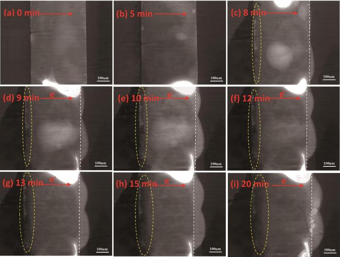
图6
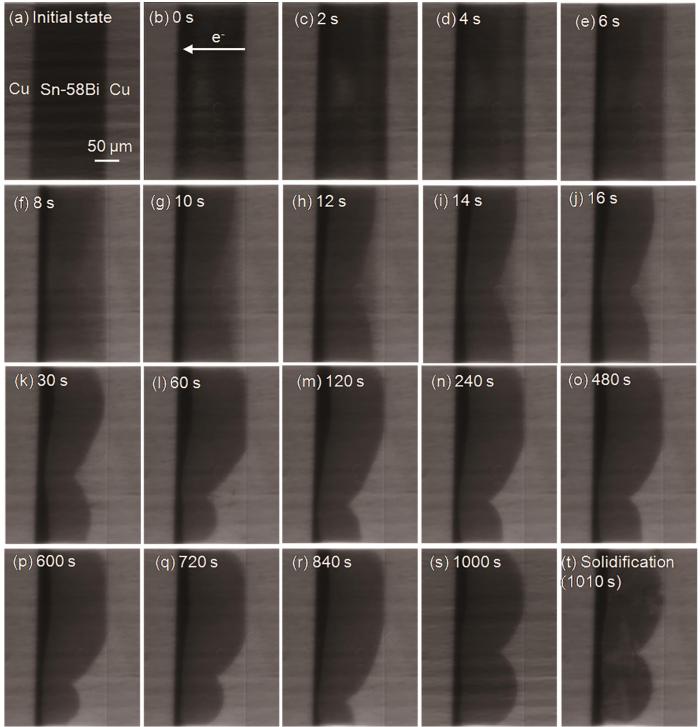
本文作者团队[46,47]利用同步辐射技术动态表征了Cu/Sn-52%In/Cu焊点的液-固电迁移行为,并与其固-固电迁移行为进行了比较。固-固电迁移过程中,由于Sn原子的|Z* |大于In原子的|Z* |,Sn原子顺电子风方向迁移至阳极形成富Sn相,在背应力作用下In原子逆电子风方向迁移至阴极形成富In相,产生两相分离现象;液-固电迁移过程中,由于不存在背应力,并且In原子的Z* 为负数(150 ℃条件下Z* = -0.6),In原子顺电子风方向朝阳极定向迁移,阳极侧生成两层较厚的Cu2(In0.45, Sn0.55)和Cu(In0.78, Sn0.22)2 IMCs,阴极侧生成两层较薄的Cu2(In0.49, Sn0.51)和Cu(In0.76, Sn0.24)2 IMCs,不同于固-固电迁移过程中产生的两相分离现象,在液-固电迁移过程中产生了极性效应现象。
张志杰和黄明亮[48]利用同步辐射技术动态表征了Cu/Sn-37%Pb/Cu焊点的液-固电迁移行为。加热阶段,Pb原子向阳极迁移并形成富Pb相;保温阶段,阳极侧富Pb相部分溶解,反向迁移至阴极,形成两相平衡组织;冷却阶段,Pb原子再次向阳极迁移,最终形成富Pb相、Sn-Pb相、富Sn相三相组织。液-固电迁移过程中Pb原子的迁移行为归因于其电迁移通量与化学势通量竞争机制。
图7
2.3 电迁移寿命评估模型
2.3.1 Black方程
微焊点的电迁移平均失效时间(mean-time-to-failure,MTTF)是评价其抗电迁移性能的重要指标,它直接关系到电子产品的服役寿命。Black方程[54]是目前最常用的描述电迁移平均失效时间的经验公式,用于预测加速实验条件直流模型下电迁移平均失效时间:
2.3.2 Black方程的修正
为了提高Black方程对微焊点电迁移寿命预测的准确度,研究人员对Black方程中的T和j进行了修正。
首先,在Joule热作用下,测试焊点处温度会高于环境温度T,此时Black方程修正为:
式中,ΔT为Joule热导致的焊点温度升高。Chen等[57]通过电阻温度系数的换算,获得了j与ΔT之间的关系,并对陶瓷封装的铜柱(Cu pillar)凸点结构和塑料封装的Cu pillar凸点结构的Black方程分别进行了修正,分别如
此外,由于微焊点特殊的几何形状,电流密度在焊点内分布并不均匀,在预测电迁移寿命时应按焊点内最大电流密度计算,则Black方程修正为[58]:
式中,λ为电流密度修正系数。Li等[58]模拟了500 μm尺寸SAC305焊点内的电流密度分布情况,发现焊点电子入口处的电流密度是整体平均电流密度的7.24倍,即λ = 7.24。
相较于直流电迁移,双脉冲电流波形的交流电迁移更加复杂。Ting等[59]通过引入损伤恢复因子(r)对交流电迁移条件下的Black方程进行了修正:
式中,
式中,
Black方程最早用于预测Al、Cu等互连导线的电迁移寿命,仅考虑了单质金属中单一原子的扩散行为。然而,芯片互连微焊点电迁移过程中需要考虑几何形状、互连结构中的多界面特征以及原子扩散之间的协同/竞争关系等多种因素。因此,Black方程在芯片互连微焊点电迁移寿命中的应用缺乏可靠的物理理论基础,目前仅作为经验公式供研究人员参考使用。
2.3.3 数值模拟在电迁移寿命评估中的应用
数值模拟已成为微焊点在电-热-力多物理场耦合实际服役条件下寿命评估中重要的研究手段。Liang等[60,61]基于相场法模拟了电迁移作用下阳极界面IMC的生长过程,发现IMC晶粒在较高电导率的方向生长速率更快。Zhao等[62]构建了电-热-力-扩散多场耦合模型,发现Cu/Sn/Cu焊点电迁移过程中空洞在阴极侧钎料与IMC的界面处形成。郭福等[63]通过数值模拟发现:电迁移通量和原子浓度梯度通量是空洞形成的主要因素,而温度循环条件下电迁移通量和应力梯度通量是空洞形成的主要因素。在数值模拟研究中,模拟结果的准确性受多种因素的影响,其中边界条件的设定和参数的选择尤为关键。边界条件的合理性决定了模拟系统的范围和约束,而参数的准确性决定了模拟过程是否能够真实反映微焊点电迁移进程。因此,优化边界条件和校准参数能够进一步提升数值模拟的准确性。
3 微凸点电迁移可靠性提升方法
微焊点的抗电迁移性能决定着电子产品的使用寿命,如何提升微焊点电迁移可靠性一直是研究人员关注的重点。本节从微焊点合金成分优化,添加增强相,凸点下金属化层的选择与组合,微焊点中β-Sn晶粒取向调控,以及制备全IMC焊点等方面综述了微焊点电迁移可靠性提升的方法。
3.1 微凸点合金成分优化
3.1.1 合金化方式提升Sn-Ag-Cu体系钎料合金微凸点电迁移可靠性
3.1.2 合金化方式提升Sn-Bi基钎料合金体系微凸点电迁移可靠性
Sn-Bi基钎料合金由于具有较低的工艺温度和优异的力学性能,已成为低温钎焊领域的主流选择。然而,其在电迁移过程中易发生Sn、Bi两相分离,导致阳极侧界面形成过厚的脆性富Bi相,对微焊点的可靠性构成严重挑战。为了应对这一挑战,研究人员通过在钎料中加入合金元素抑制电迁移过程中富Bi层的形成速率,进而提高Sn-Bi钎料焊点抗电迁移性能。研究[70]发现:在Sn-Bi钎料中加入Ag元素,能够在焊点内形成Ag3Sn IMC颗粒,降低电迁移过程中Bi原子的迁移速率。在Sn-Bi钎料中加入少量Ni元素,会在焊点内形成NiBi3金属间化合物,同样可以降低Bi原子的迁移速率。此外,还可以在Sn-Bi钎料中加入Ge元素,Ge元素分布在Bi相内部或在相界处,抑制了电迁移过程中Bi原子的迁移,从而降低富Bi相的生长速率[71]。Wu等[72,73]研究发现,在Sn-58%Bi钎料中添加Sb元素能够促进Bi相中孪晶的形成,形成的孪晶可以抑制电迁移与温度循环耦合作用下的局部变形,从而提高焊点的可靠性。
3.2 添加增强相方式提升微凸点钎料合金电迁移可靠性
除了通过合金化向钎料添加合金元素外,在钎料合金焊膏中混入金属颗粒、非金属颗粒、碳材料等增强相,在回流过程中形成复合钎料焊点,也是提升焊点抗电迁移性能的重要研究方向。
3.3 UBM选择与组合
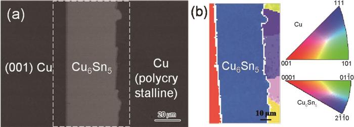
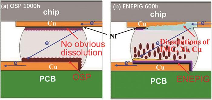
相较于Cu UBM (包括有机可焊性保护层(organic solderability preservative,OSP)、Cu pillar等)、Ni UBM (包括化学镀镍浸金(electroless nickel/immersion gold,ENIG)、化学镀镍钯浸金(electroless nickel electroless palladium immersion gold,ENEPIG)等)在电迁移过程中表现出良好的抗电迁移性能[85~87],可以用作扩散阻挡层抑制Cu原子向钎料内扩散,减缓阳极侧界面IMC的生长速率,抑制阴极侧UBM的过度溶解,提高互连微焊点的抗电迁移性能。同时,互连焊点两侧基板的交互作用对焊点的电迁移可靠性有显著影响。本文作者团队[88]在研究Ni/SAC305/UBM焊点的电迁移行为时发现,相比于ENEPIG表面处理层,采用OSP作为UBM层时,印制电路板(PCB)侧Cu基体的溶解导致芯片侧界面形成更高稳定性的(Cu, Ni)6Sn5型金属间化合物,抑制了电迁移过程中芯片侧Ni UBM的溶解,从而显著提高了焊点的电迁移可靠性,如图8[88]所示。相较于Cu/solder/Cu和Ni/solder/Ni对称结构焊点,Cu/solder/Ni的非对称结构焊点具有更高的抗电迁移性能。
图8
为提高Cu UBM基体的抗电迁移性能,研究人员通过向Cu基体中添加适量的Zn元素来提高UBM基体的抗电迁移性能,Cu-Zn合金替代Cu作为UBM层能够避免因阴极Cu基体溶解而导致的电迁移失效,减缓了电迁移过程中界面空洞的形成速率,延长SAC305焊点的电迁移寿命。Wang等[89]采用Cu-4.89%Zn代替Cu作为焊点的UBM层,能够阻碍阳极侧Sn晶须和阴极侧空洞的形成,同时还可以抑制阳极侧富Bi相的生长,提高了Sn-58%Bi钎料焊点的电迁移寿命。Cu-Zn UBM虽然提高了焊点的抗电迁移性能,但是Zn原子在界面反应过程中溶解进入钎料会降低微焊点的抗氧化性能,限制了其在电子封装领域的应用。
(111)择优取向纳米孪晶Cu (nano-twinned Cu,nt-Cu)可以通过低成本电镀方式制备,工艺方法简单,与目前封装工艺兼容度高,受到广泛关注。(111) nt-Cu基体由垂直于表面的柱状晶组成,同时每一个柱状晶内存在大量平行于基体表面的孪晶界,孪晶界与柱状晶界处形成的三叉点(triple point)能够抑制Cu原子的扩散。本文作者团队[90]在针对(111) nt-Cu UBM的电迁移可靠性研究中发现:(111) nt-Cu UBM作为阴极时的溶解速率比多晶Cu作为阴极时的溶解速率低20%,表现出更好的抗电迁移性能。然而也有研究[91]认为(111)晶面Cu原子具有更大活性,相比于多晶Cu UBM,(111) nt-Cu UBM中存在大量晶界,为Cu原子的扩散和溶解提供了更多通道,加速了其作为阴极时的溶解速率。(111) nt-Cu在不同条件下的电迁移行为特征可能受到多种因素的综合影响,需进一步深入研究。
3.4 微凸点中 β-Sn晶粒晶体取向调控
β-Sn晶粒的各向异性显著影响了互连微焊点的电迁移失效模式,研究人员从多方面着手,通过改变钎料合金成分、外加磁场以及外延生长等方法调控β-Sn晶粒的晶体取向,以提升微焊点电迁移可靠性。
研究发现:钎料中Ag元素的含量对β-Sn晶粒的晶体取向有很大影响。Chen等[92]在针对不同Ag含量的钎料焊点中β-Sn晶粒的晶体取向研究中发现:当Ag含量大于3%时,β-Sn晶粒的c轴方向倾向于平行基板方向(垂直于电流方向),可以抑制微焊点电迁移失效;当Ag含量小于2%时,β-Sn晶粒的c轴方向垂直于平行基板方向(平行于电流方向),将加速微焊点电迁移失效。
通过提高钎料中Ag元素含量或在凝固过程中外加磁场都可以获得c轴与电迁移方向平行的β-Sn晶粒。然而,过高的Ag含量增加了钎料中大片状Ag3Sn相的析出概率,恶化了焊点力学性能;外加磁场会对电子元器件造成影响,很难在实际生产中应用。
图9
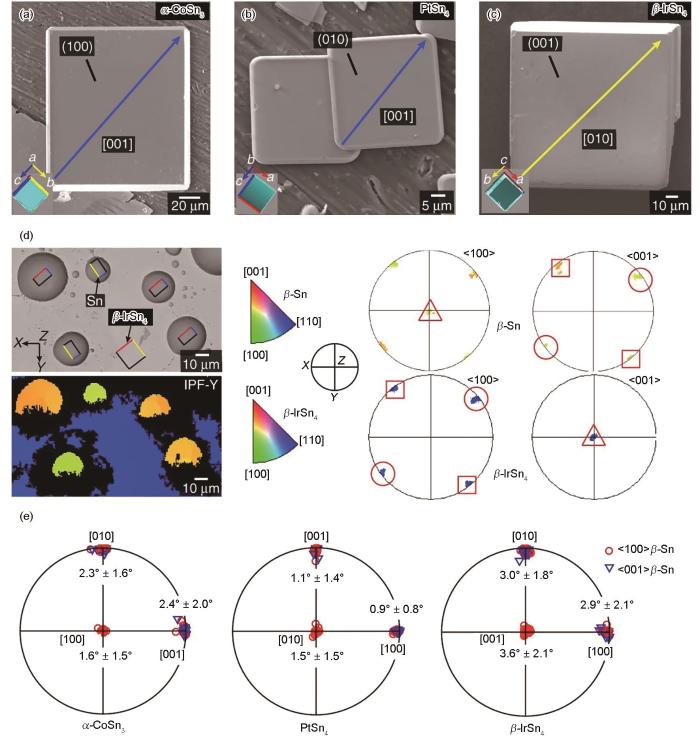
图9
通过Sn在单晶IMC片上形核凝固调控β-Sn晶粒取向[95]
Fig.9
Nucleation of Sn droplets on the facets of single-crystal IMCs[95]
(a-c) typical α-CoSn3, PtSn4, and β-IrSn4 single crystals, respectively
(d) a typical example of Sn droplets solidified on the (001) facet of β-IrSn4
(e) summarized pole figures of β-Sn orientations with respect to the largest facets of α-CoSn3, PtSn4, and β-IrSn4
3.5 微型化趋势下全金属间化合物焊点设计与制备
通过在钎料中加入适量的合金元素或增强相来提高焊点的电迁移可靠性是目前最常用的解决思路。一方面,通过加入的合金元素/增强相抑制电迁移过程中极性效应引发的界面IMC的过度生长;另一方面,这些合金元素/增强相的添加还能抑制钎料内部因电迁移造成的元素偏聚。然而,在考虑电迁移可靠性的同时,合金元素/增强相的添加还需要综合考虑钎料润湿性、工艺性能与力学性能等多方面因素,并针对特定应用场景采取相应的解决方案。UBM类型的选择和组合是一个较为简单可行的提高微焊点抗电迁移性能的方法。β-Sn晶粒晶体取向的调控可以有效提高锡基微焊点电迁移可靠性,然而目前的研究主要局限在实验室对单个或少量凸点的调控,还难以大规模应用到生产实践中。全IMC焊点设计与制备符合微型化的发展趋势,是未来提升微小尺度焊点电迁移可靠性的发展方向。
4 总结与展望
引领芯片技术发展的“摩尔定律”正面临着接近自身物理极限,先进封装技术中芯片锡基微凸点的尺寸持续减小至微米级别,通过微凸点的电流密度达到1 × 10⁴ A/cm2,导致电迁移已成为芯片锡基微凸点的重要可靠性问题。低熔点、微尺度、多材料、多界面、交互作用等特征使电迁移研究的复杂性增加,其可靠性面临严峻挑战。本文综述了锡基微凸点电迁移的物理本质、主要影响因素、研究方法、电迁移行为特征及寿命评估模型的研究进展,总结了锡基微凸点电迁移可靠性提升方法,旨在指导优化电迁移的可靠性设计。
(1) 电流密度、焊点温度、β-Sn晶粒各向异性及多物理场耦合作用是影响微焊点电迁移可靠性的主要因素。电流拥挤效应使微焊点电流出入口处的局部电流密度急剧升高,加速电迁移失效;温度显著影响扩散系数D (金属原子在液相中的扩散系数比固相中高几个数量级,液-固电迁移速率远高于固-固电迁移速率)和有效电荷数Z* 等,决定了主要扩散原子类型和微焊点电迁移失效速率;β-Sn晶粒c轴方向与电子运动方向夹角越小,阴极基体溶解速率越快,微焊点电迁移寿命越短;电-热-力多物理场耦合的实际服役条件最终决定了微焊点的电迁移寿命。
(2) 电迁移过程中金属原子的扩散方向和扩散速率由参数Z* 、D以及扩散原子竞争关系控制,导致锡基微凸点中表现出不同的电迁移特征:极性效应表现为金属原子从阴极向阳极定向迁移,导致阴极UBM基体和界面IMC的溶解以及阳极界面IMC的生长增厚;反极性效应表现为少数金属原子(目前仅发现Zn原子)从阳极向阴极定向迁移,导致阴极界面IMC的生长增厚;两相分离表现为Sn-Bi、Sn-In、Sn-Pb等微焊点中Sn原子与另一种金属原子分别向阴极和阳极定向迁移,最终产生两相分离现象。
(3) 目前Black方程是最常用的微焊点电迁移寿命评估模型,但是基于单质Al、Cu等互连导线所建立的Black方程无法精确预测微焊点的电迁移寿命,这是由于微焊点几何形状、多界面结构以及电迁移过程中原子扩散协同/竞争机制等因素均影响微焊点的电迁移寿命。尽管通过修正温度T和电流密度j等参数可有限提升Black方程的准确度,但仍存在较大的局限性。更加准确的电迁移寿命评估模型需根据微焊点实际失效模式与失效机理,并结合数值模拟构建相应的电迁移损伤物理与数学模型,从而实现微焊点电迁移寿命的精确预测。
(4) 微焊点电迁移可靠性提升方法主要包括:通过改变钎料合金成分,在晶界处析出IMC颗粒,抑制电迁移过程中金属原子的定向迁移;向钎料合金中掺杂增强相,降低电迁移过程中金属原子的迁移速率;制备具有特殊组织结构(如(111)孪晶)或特殊合金成分的UBM基体,或者通过两侧UBM基体的交互作用形成更稳定的界面IMC层,进而抑制电迁移过程中阴极UBM基体的溶解;通过改变钎料合金成分、外加磁场以及外延生长等方法调控β-Sn晶粒晶体取向,降低电迁移过程中阴极UBM基体的溶解速率;全IMC焊点,其具有优异的抗电迁移性能。上述方法从不同角度提高了微焊点的抗电迁移性能,为电迁移可靠性设计提供了新的思路和方法。
随着先进封装技术向微型化、高性能化方向持续发展,芯片互连锡基微凸点电迁移可靠性面临更大的挑战,电迁移未来研究方向主要包括:
(1) 深入探究“电-热-力”多物理场耦合作用下微焊点的电迁移失效机理将是未来的重点研究方向。
(2) β-Sn晶粒晶体取向的调控是提高锡基微焊点电迁移可靠性的关键技术手段之一,如何将实验室受到局限的β-Sn晶粒取向调控技术大规模应用到生产实践中是未来的研究方向。
(3) 新型择优取向纳米孪晶Cu具有特殊的组织结构,可有效降低电迁移过程中Cu基体的溶解速率,但是其作为UBM制备的微焊点的电迁移可靠性机理仍需系统研究。
(4) 金属原子的扩散通量是理解微焊点电迁移失效机理的关键点,结合多场耦合作用下的数值模拟,基于金属原子的扩散通量建立典型芯片互连微焊点结构和服役环境下的微焊点电迁移寿命预测模型(取代目前常用的经验公式Black方程),以及相应的可靠性分析方法与评价标准,实现芯片互连微焊点电迁移寿命的精准预测。
参考文献
De l'action de la pile sur les sels de potasse st de soude st sur les alliages soumis à la fusion ingée
[J].
Direct transmission electron microscope observation of electrotransport in aluminum thin films
[J].
Modeling electromigration-induced stress evolution in confined metal lines
[J].
Electromigration studies of flip chip bump solder joints
[A].
Recent advances on electromigration in very-large-scale-integration of interconnects
[J].
Investigation of the temperature dependence in Black's equation using microscopic electromigration modeling
[J].
Interfacial intermetallic compound modification to extend the electromigration lifetime of copper pillar joints
[J].
Effects of trace elements Ag, Bi and Ni on solid-liquid electromigration interface diffusion in solder joints
[J].
An in-situ experimental and simulation study on the electromigration behavior of SAC305 solder joints
[J].
Failure mechanisms of Ni/Sn-3.0Ag-0.5Cu/OSP flip chip solder under high current stressing
[A].
Effect of electromigration on intermetallic compound formation in Cu/Sn/Cu interconnect
[A].
Electromigration behaviors in Sn-58Bi solder joints under different current densities and temperatures
[J].
In situ study on reverse polarity effect in Cu/Sn-9Zn/Ni interconnect undergoing liquid-solid electromigration
[J].
A synchrotron radiation real-time in situ imaging study on the reverse polarity effect in Cu/Sn-9Zn/Cu interconnect during liquid-solid electromigration
[J].
Study on liquid-solid electromigration in Cu/Sn-9Zn/Cu interconnect using synchrotron radiation real-time in situ imaging technology
[A].
Reverse polarity effect and cross-solder interaction in Cu/Sn-9Zn/Ni interconnect during liquid-solid electromigration
[J].
Cu-Ni cross-solder interaction in Cu/Sn-58Bi/Ni interconnect undergoing liquid-solid electromigration
[J].
Cu/Sn-58Bi/Ni焊点液-固电迁移下Cu和Ni的交互作用
[J].
Abnormal migration behavior and segregation mechanism of Bi atoms undergoing liquid-solid electromigration
[J].
The migration behavior of Bi atoms in Cu/Sn-58Bi/Cu solder interconnects undergoing liquid-solid electromigration (L-S EM) was in situ observed using synchrotron radiation real-time imaging technology. Bi atoms tend to migrate from the cathode toward the anode resulting in the linear growth of Bi-rich phase layer at the anode in both the heating and cooling stages but not in the dwelling stage. Since the temperature of Sn-Bi solder in the dwelling stage is higher than those in both the heating and cooling stages, the electrically driven migration effect diminishes with increasing temperature. As a result, a three-layer equilibrium distribution of Bi-rich, Sn-Bi and Sn-rich phases across the solder is observed in the dwelling stage of 140 degrees C, and a uniform Bi distribution across the solder is observed in the dwelling stage of a higher temperature of 170 degrees C, i.e., Bi atoms fully diffuse backward at such a high temperature. The abnormal migration behavior of Bi atoms is determined by the combined effect of chemical potential gradient-induced flux (J(chem)) and EM-induced flux (J(em)). The EM-induced flux (J(em)) is determined by the effective charge number (Z*) of Bi atoms that is calculated as - 3.57 at 140 degrees C based on the growth kinetics of the Bi-rich layer. Furthermore, the Z* value of Bi atoms is calculated as - 3.04 by using a modified model for calculating Z* of liquid metals, which agrees well with the experimental value. The present work provides a reference for purifying refractory metals from alloys.
In situ observation of electromigration-induced anomalous precipitation of Ag3Sn phase in Ag-containing solder joints
[J].
Effect of electromigration on intermetallic compound formation in line-type Cu/Sn/Cu and Cu/Sn/Ni interconnects
[A].
Liquid-solid electromigration behavior and mechanism of micro interconnect
[D].
微互连焊点液-固电迁移行为与机理研究
[D].
Role of diffusion anisotropy in β-Sn in microstructural evolution of Sn-3.0Ag-0.5Cu flip chip bumps undergoing electromigration
[J].
Interaction between β-Sn grain orientation and electromigration behavior in flip-chip lead-free solder bumps
[J].
倒装芯片无铅凸点β-Sn晶粒取向与电迁移交互作用
[J].采用原位电迁移实验研究了在150 ℃、1.0×10<sup>4</sup> A/cm<sup>2</sup>条件下倒装芯片Ni/Sn-3.0Ag-0.5Cu/Ni-P无铅凸点中β-Sn晶粒取向对金属间化合物(IMC)的聚集析出机制、阴极Ni芯片侧(UBM)溶解行为、电迁移失效机制以及电迁移驱动下β-Sn晶粒的旋转滑移机制的影响。原位观察发现,电迁移过程中(Ni, Cu)<sub>3</sub>Sn<sub>4</sub>类型IMC在凸点中仅沿着β-Sn晶粒的c轴方向析出,且倾向于在θ角(β-Sn晶粒的c轴与电子流动方向之间的夹角)较小的晶粒内析出;同时,阳极附近观察到β-Sn挤出现象,即凸点出现应力松弛。建立了阴极Ni UBM溶解量与β-Sn晶粒取向的关系模型:β-Sn晶粒取向决定阴极Ni UBM的溶解量,即当θ角很小时,Ni UBM会出现明显溶解;当θ角增大时,Ni UBM的溶解受到抑制,该模型与实验值基本吻合。电迁移导致β-Sn晶粒发生旋转滑移,认为是由于不同取向的相邻β-Sn晶粒中电迁移导致的空位通量不同,从而导致阳极晶界处于空位的过饱和,阴极晶界处于空位的未饱和状态,并促使空位沿着晶界出入于自由表面,最终在垂直方向上会产生空位梯度,由沿晶界的空位梯度对应的应力梯度产生的力矩使β-Sn晶粒发生旋转滑移。
Dominant effect of high anisotropy in β-Sn grain on electromigration-induced failure mechanism in Sn-3.0Ag-0.5Cu interconnect
[J].
The effect of grain orientation of β-Sn on copper pillar solder joints during electromigration
[J].
Detrimental angle range between c axis of Sn crystal and electron flow for the electromigration reliability of ball grid array devices
[J].
Effect of Sn grain c-axis on Cu atomic motion in Cu reinforced composite solder joints under electromigration
[J].
Role of crystallographic orientation of β-Sn grain on electromigration failures in lead-free solder joint: An overview
[J].
Effect of Sn grain orientation on reliability issues of Sn-rich solder joints
[J].
Revealing evolutions of intermetallics in a solder joint under electromigration: A quasi-in situ study combining 3D microstructural characterization and numerical simulation
[J].
Control of solder microstructure stimulated by interface condition of the UBM/solder and enhancement of electromigration reliability
[A].
Single-grain Sn-rich micro-bump by reducing Sn undercooling with heterogeneous nucleation
[J].
A case study of intermetallic evolutions in a solder joint under electromigration using a novel experiment-simulation combined approach
[A].
The Evolution of micro-voids in Sn37Pb solder joints under electromechanical coupling loading
[J].
Thermal cycling-electric current coupling damage mechanisms of SnAgCu/Cu solder joints under different temperature ranges
[J].
Current-induced solder evolution and mechanical property of Sn-3.0Ag-0.5Cu solder joints under thermal shock condition
[J].
Effect of electroless Ni-P consumption on the failure mechanism of solder joints during electromigration
[J].<p>The consumption of electroless Ni-P and its effect on the failure mechanism of solder joints duringelectromigration under a current density of 1.0×<span>10<sup>4</sup> A/cm<sup>2</sup> at both 150 and 200℃ wereinvestigated using line-type Cu/Sn/Ni-P solder joints. Before the electroless Ni-P was completely consumed,the microstructural evolution of the Sn/Ni-P interface (cathode) was the formation of Ni<sub>2</sub>SnP and Ni<sub>3</sub>P accompanied by the consumption of the electroless Ni-P. Ni atoms diffused from the electroless Ni--P into the Sn solder under electron current stressing. Most Ni atoms precipitated as (Cu, Ni)<sub>6</sub>Sn<sub>5</sub> or (Ni, Cu)<sub>3</sub>Sn<sub>4</sub> in the Sn solder, and few Ni atoms could arrive at the opposite Cu/Sn interface (anode). After the electroless Ni-P was completely consumed, the microstructural evolutions of the Sn/Ni-P interface (cathode) were the formation of voids and the transformation from Ni<sub>3</sub>P to Ni<sub>2</sub>SnP. Furthermore, cracks that resulted from the propagation of voids significantly increased the current density through solder joints, and thus greatly enhanced the Joule heating of solder joints, resulting in the failure of solder joints by the fusing of Sn solder.</span></p><div style="line-height: 150%"> </div>
Ni-P消耗对焊点电迁移失效机理的影响
[J].研究了Cu/Sn/Ni--P线性焊点在150和200 ℃, 电流密度1.0×10<sup>4</sup> A/cm<sup>2</sup>的条件下化学镀Ni--P层消耗及其对焊点失效机理的影响. 结果表明, 在Ni-P层完全消耗之前, 阴极界面的变化表现为: 伴随着Ni--P层的消耗, 在Sn/Ni-P界面上生成Ni<sub>2</sub>SnP和Ni<sub>3</sub>P; 从Ni-P层中扩散到钎料中的Ni原子在钎料中以(Cu, Ni)<sub>6</sub>Sn<sub>5</sub>或(Ni, Cu)<sub>3</sub>Sn<sub>4</sub>类型的IMC析出, 仅有很少量的Ni原子能扩散到对面的Cu/Sn阳极界面. 当Ni--P层完全消耗后, 阴极界面的变化主要表现为: 空洞在Sn/Ni<sub>2</sub>SnP界面形成, Ni<sub>3</sub>P逐渐转变为Ni<sub>2</sub>SnP, 空洞进一步展形成裂缝, 从而导致通过焊点的实际电流密度升高、产生的Joule热增加, 最终导致焊点发生高温电迁移熔断失效.
Influence of temperature and current stressing on Cu-Sn intermetallic compound growth characteristics of lead-free microbump
[J].
Polarity effect of interfacial intermetallic compounds of BGA structure Cu/Sn-52In/Cu solder joints during electromigration
[J].
Effect of electromigration on intermetallic compound formation in line-type Cu/Sn/Cu interconnect
[J].
Reverse polarity effect from effective charge disparity during electromigration in eutectic Sn-Zn solder interconnect
[J].
Study on phase electromigration and segregation behavior of Cu-cored Sn-58Bi solder interconnects under electric current stressing
[J].
Effect of electromigration on microstructure and properties of CeO2 nanopartical-reinforced Sn58Bi/Cu solder joints
[J].
Current-induced phase partitioning in eutectic indium-tin Pb-free solder interconnect
[J].
Migration behavior of indium atoms in Cu/Sn-52In/Cu interconnects during electromigration
[J].
Liquid-solid electromigration behavior of Cu/Sn-52In/Cu micro-interconnect
[J].Electromigration (EM), which describes the mass transport due to the momentum exchange between conducting electrons and diffusing metal atoms under an applied electric field, has become a serious reliability issue in high-density packaging. With the increasing demands for miniaturization, liquid-solid (L-S) EM will pose a critical challenge to the reliability of solder interconnects. In this work, The interfacial reactions and diffusion behaviors of In, Sn and Cu atoms in Cu/Sn-52In/Cu interconnects during L-S EM under a current density of 2.0×10⁴ A/cm2 at 120 and 180 ℃ have been in situ studied by using synchrotron radiation real-time imaging technology. During L-S EM, since there was no back-stress, the In atoms directionally migrated toward the anode due to the negative effective charge number (Z*) of In, which is different from the In atoms directionally migrated toward the cathode due to the back-stress induced by the preferential migration of the Sn atoms over the In atoms toward the anode during the solid-solid (S-S) EM. Furthermore, a modified expression for calculating the effective charge number Z* of liquid metals was proposed based on the enthalpy changes of melting process. The Z* of In atoms was calculated to be -2.30 and -1.14 at 120 and 180 ℃, respectively, which was consistent with the migration behavior of In atoms. The model provides a theoretical basis for determining the direction of the EM. The polarity effect, evidenced by the IMC layer at the anode growing continuously while that at the cathode was restrained, was resulted from the directional migration of In and Cu atoms toward the anode during L-S EM, which was more significant at high temperature. The consumption of cathode Cu during L-S EM followed a parabolic relationship with the EM time, and the consumption rate was magnitude higher at high temperature. The migrations of In atoms was discussed in terms of diffusion flux.
Cu/Sn-52In/Cu微焊点液-固电迁移行为研究
[J].采用同步辐射实时成像技术对比研究了Cu/Sn-52In/Cu微焊点在120和180 ℃,2.0×10<sup>4</sup> A/cm<sup>2</sup>条件下液-固电迁移过程中In、Sn和Cu原子的扩散迁移行为及其对界面反应的影响。由于没有背应力,液-固电迁移条件下Sn-52In焊点中In原子的有效电荷数Z<sup>*</sup>为负值是其定向扩散迁移至阳极的物理本质,这与Sn-52In焊点固-固电迁移条件下背应力驱使In原子迁移至阴极的机理不同。基于液态金属焓随温度的变化关系,修正了计算液态金属Z<sup>*</sup>的理论模型,计算获得In原子在120和180 ℃下的Z<sup>*</sup>分别为-2.30和-1.14,为电迁移方向提供了判断依据。液-固电迁移过程中In和Cu原子同时由阴极扩散至阳极并参与界面反应使得界面金属间化合物(intermetallic compounds,IMC)生长表现为“极性效应”,即阳极界面IMC持续生长变厚,并且厚于阴极界面IMC,温度越高,界面IMC的“极性效应”越显著。液-固电迁移过程中阴极Cu基体的溶解与时间呈抛物线关系,温度越高,阴极Cu的溶解速率越快。
In situ study on liquid-solid electromigration behavior in Cu/Sn-37Pb/Cu micro-interconnect
[J].Electromigration (EM), which describes the mass transport due to momentum exchange between conducting electrons and diffusing metal atoms under an applied electric field, has become a serious reliability issue in high-density packaging. With the increasing demands for miniaturization, liquid-solid (L-S) EM will pose a critical challenge to the reliability of solder interconnects. In this work, synchrotron radiation real-time imaging technology is used to in situ study the interfacial reaction and atom migration in Cu/Sn-37Pb/Cu solder interconnects undergoing L-S EM at 185 ℃ with a current density of 1.0×10⁴ A/cm2. In the heating stage, Pb atoms directionally migrate from the cathode toward the anode, resulting in the growth of Pb-rich phase at the anode. In the dwelling stage, Pb atoms diffuse backward, then equilibrium phase is obtained. In the cooling stage, Pb atoms directionally migrate from the cathode toward the anode again until the solder solidified, three phases is obtained: the Pb-rich phase, the Sn-Pb phase and the Sn-rich phase. The abnormal migration behavior of Pb atoms in different stages is determined by the combined effect of the chemical potential gradient flux (Jchem) and EM-induced flux (Jem). Jem is determined by the effective charge number (Z*) of Pb atoms, which was calculated to be -3.20 at 185 ℃ based on the growth kinetics of the Pb-rich layer model.
原位研究Cu/Sn-37Pb/Cu微焊点液-固电迁移行为
[J].利用同步辐射实时成像技术原位研究了Cu/Sn-37Pb/Cu微焊点在185 ℃、1×10<sup>4</sup> A/cm<sup>2</sup>电流密度条件下液-固电迁移过程中Pb原子的扩散迁移行为及其析出机制。在微焊点加热熔化阶段,Pb原子向阳极定向迁移并聚集形成富Pb相,其厚度随时间的延长而增大;在保温阶段,阳极的富Pb相部分溶解,Pb原子反向扩散至阴极,最终钎料内部形成两相平衡组织;在冷却凝固阶段,Pb原子再次向阳极定向迁移,直至凝固,最终钎料内部形成三相组织:富Pb相、Sn-Pb相和富Sn相。基于加热阶段富Pb相的生长动力学,计算获得Pb原子在185 ℃下的有效电荷数(Z<sup>*</sup>)为-3.20,为Pb原子的电迁移方向提供了判断依据。Pb原子在电迁移中的反常迁移行为归因于电迁移通量(J<sub>em</sub>)与化学势通量(J<sub>chem</sub>)的竞争机制。
Novel growth of whole preferred orientation intermetallic compound interconnects for 3D IC packaging
[A].
Electromigration behavior and mechanical properties of the whole preferred orientation intermetallic compound interconnects for 3D packaging
[A].
Effects of electromigration on microstructural evolution and mechanical properties of preferential growth intermetallic compound interconnects for 3D packaging
[A].
A preparation method and structure of full intermetallic compound (IMC) interconnects
[P].
一种全金属间化合物互连焊点的制备方法及结构
[P].
A method to control crystal orientation and microstructure of full intermetallic compound (IMC) interconnects
[P].
一种控制全金属间化合物微互连焊点晶体取向及微观组织的方法
[P].
Electromigration failure modes in aluminum metallization for semiconductor devices
[J].
Influence of Sn grain orientation on mean-time-to-failure equation for microbumps in 3D IC technology
[J].
Changes in the microstructure and electrical resistance of SnBi-based solder joints during current stressing
[J].
Black equation of the electromigration lifetime for ceramic package with lead bumps and plastic package with lead-free bump
[A].
A study on the effects of electrical and thermal stresses on void formation and migration lifetime of Sn3.0Ag0.5Cu solder joints
[J].
AC electromigration characterization and modeling of multilayered interconnects
[A].
Insight into the preferential grain growth of intermetallics under electric current stressing—A phase field modeling
[J].
Phase field modelling combined with data-driven approach to unravel the orientation influenced growth of interfacial Cu6Sn5 intermetallics under electric current stressing
[J].
Competitive failure mechanism and load tolerance of solder joint under thermo-mechano-electrical coupling
[J].
Electromigration damage analysis of BGA solder joint under high temperature and high current density
[J].
高温高电流密度下BGA焊点电迁移损伤
[J].
Effects of bismuth additions on mechanical property and microstructure of SAC-Bi solder joint under current stressing
[J].
Tin whiskers formation in Sn0.7Cu0.05Ni1.5Bi under electro-migration stressing
[J].
Effect of Ag additives on the consumption of a cathode Cu pad in a Cu/Sn3.5Ag/Cu flip-chip structure under electromigration
[J].
Effects of Zn addition on electromigration behavior of Sn-1Ag-0.5Cu solder interconnect
[J].
Electromigration behavior of low-silver Sn-0.3Ag-0.7Cu-1.6Bi-0.2In solder joints
[J].
Effect of trace addition of In on Sn-Cu solder joint microstructure under electromigration
[J].
Electromigration behavior of Cu/Sn-58Bi-1Ag/Cu solder joints by ultrasonic soldering process
[J].
Electromigration behaviors and effects of addition elements on the formation of a Bi-rich layer in Sn58Bi-based solders
[J].
Microstructural evolution of joints with and without Sb, Ni in Sn58Bi solder under electro-thermal-force coupling
[J].
Mechanical properties and microstructure evolution of Sn-Bi-based solder joints by microalloying regulation mechanism
[J].
Effect of Zn nanoparticle-doped flux on mechanical properties of SAC305 solder joint after electromigration
[J].
Grain size stability of interfacial intermetallic compound in Ni and Co nanoparticle-doped SAC305 solder joints under electromigration
[J].
Effect of cobalt doping on the microstructure and tensile properties of lead free solder joint subjected to electromigration
[J].Rapid Cu diffusion is one of the main causes of electromigration (EM) failure in lead-free solder joints. In this study, an effort has been made to investigate the detrimental effects of EM on microstructure and mechanical performance of solder joint by introducing Co nanoparticles (NP) doped flux at the interface between SAC305 solder and copper substrate. EM tests were conducted on un-doped SAC305 and Co-doped SAC305 solder joints for different time intervals, with the maximum duration of 1128 h. A DC current was applied to the both types of solder joints to achieve a current density of 1 × 10⁴ A/cm2. EM tests were performed in an oil bath maintained at a constant temperature of 80 °C. It is found that Co-doped flux significantly reduced the formation of cracks and voids at the cathode interface. Co atoms entered into the lattice of Cu6Sn5 leading to the formation of (Cu, Co)6Sn5. This thermodynamically stabilized the interfacial intermetallic (IMC) layers both at the anode and cathode sides and suppressed the change in their thickness. The average anodic growth rate of (Cu, Co)6Sn5 interfacial IMC in the doped sample was about one order of magnitude lower compared with that of Cu6Sn5 in the un-doped samples. Co-NP also improved the tensile strength considerably before and after EM. The report suggests that the reliability of solder joint during EM can be improved by using Co-NP doped flux.
Improving the mechanical performance of Sn57.6Bi0.4Ag solder joints on Au/Ni/Cu pads during aging and electromigration through the addition of tungsten (W) nanoparticle reinforcement
[J].
Electro-migration study of nano Al doped lead-free Sn-58Bi on Cu and Au/Ni/Cu ball grid array (BGA) packages
[A].
Improved electro-migration resistance in nano Ag modified Sn-58Bi solder joints under current stressing
[A].
Refinement of the microstructure of Sn-Ag-Bi-In solder, by addition of SiC nanoparticles, to reduce electromigration damage under high electric current
[J].
Electromigration reliability for Al2O3-reinforced Cu/Sn-58Bi/Cu composite solder joints
[J].
Interfacial intermetallic growth and mechanical properties of carbon nanotubes reinforced Sn3.5Ag0.5Cu solder joint under current stressing
[J].
The study on reliability of Ni-coated graphene doped SAC305 lead-free composite solders under high current-density stressing
[J].
Electromigration behaviors of Sn58%Bi solder containing Ag-coated MWCNTs with OSP surface finished PCB
[J].
Research on reliability of Ni/Sn/Cu(Ni) copper pillar bump under thermoelectric loading
[J].
Applications of Ni and Ag metallizations at the solder/Cu interfaces in advanced high-power automobile interconnects: An electromigration study
[J].
Effect of Ni(P) thickness in Au/Pd/Ni(P) surface finish on the electrical reliability of Sn-3.0Ag-0.5Cu solder joints during current-stressing
[J].
Effect of surface finish (OSP and ENEPIG) on failure mechanism induced by electromigration in Sn-3.0Ag-0.5Cu flip chip solder interconnect
[A].
Microstructural evolution of Sn-58Bi/Cu joints through minor Zn alloying substrate during electromigration
[J].
In-situ observation on liquid-solid electromigration behavior of (111) nt-Cu/Sn/Cu interconnects
[A].
Effect of (111) oriented nanotwinned Cu substrate on the electromigration of Sn58Bi solder joint at high current density
[J].
Correlation between Ag content and Cu pad consumption in lead-free solder joints under electron current stressing
[A].
Effect of magnetic flux density on Sn crystallographic orientation in a solder joint system
[J].
Magnetic-field induced anisotropy in electromigration behavior of Sn-Ag-Cu solder interconnects
[J].
Harnessing heterogeneous nucleation to control tin orientations in electronic interconnections
[J].While many aspects of electronics manufacturing are controlled with great precision, the nucleation of tin in solder joints is currently left to chance. This leads to a widely varying melt undercooling and different crystal orientations in each joint, which results in a different resistance to electromigration, thermomechanical fatigue, and other failure modes in each joint. Here we identify a family of nucleants for tin, prove their effectiveness using a novel droplet solidification technique, and demonstrate an approach to incorporate the nucleants into solder joints to control the orientation of the tin nucleation event. With this approach, it is possible to change tin nucleation from a stochastic to a deterministic process, and to generate single-crystal joints with their c-axis orientation tailored to best combat a selected failure mode.
Size effect model on kinetics of interfacial reaction between Sn-xAg-yCu solders and Cu substrate
[J].The downsizing of solder balls results in larger interfacial intermetallic compound (IMC) grains and less Cu substrate consumption in lead-free soldering on Cu substrates. This size effect on the interfacial reaction is experimentally demonstrated and theoretically analyzed using Sn-3.0Ag-0.5Cu and Sn-3.5Ag solder balls. The interfacial reaction between the Sn-xAg-yCu solders and Cu substrates is a dynamic response to a combination of effects of interfacial IMC growth, Cu substrate consumption and composition variation in the interface zone. A concentration gradient controlled (CGC) kinetics model is proposed to explain the combined effects. The concentration gradient of Cu at the interface, which is a function of solder volume, initial Cu concentration and reaction time, is the root cause of the size effect. We found that a larger Cu concentration gradient results in smaller Cu6Sn5 grains and more consumption of Cu substrate. According to our model, the growth kinetics of interfacial Cu6Sn5 obeys a t(1/3) law when the molten solder has approached the solution saturation, and will be slower otherwise due to the interfering dissolution mechanism. The size effect introduced in this model is supported by a good agreement between theoretical and experimental results. Finally, the scope of application of this model is discussed.
Scaling effect of interfacial reaction on intermetallic compound formation in Sn/Cu pillar down to 1 μm diameter
[J].
Electromigration induced failure on lead-free micro bumps in three-dimensional integrated circuits packaging
[J].
Effect of Sn grain orientation on formation of Cu6Sn5 intermetallic compounds during electromigration
[J].
A new failure mechanism of electromigration by surface diffusion of Sn on Ni and Cu metallization in microbumps
[J].
