High-energy particle irradiation can often cause microstructure damage, resulting in different types of defects in metal-based structured materials. These irradiation-induced defects can accumulate and evolve, leading to the deformation and reduction of the structural integrity of the materials. Finally, this causes the degradation of the mechanical and physical properties of the aforementioned materials. These defects can be shielded, absorbed, and annihilated by introducing interfaces in materials, alleviating the radiation damage. In the previous two decades, metal-based nanostructured materials have attracted considerable attention in designing irradiation-resistant materials because of its high density of internal interfaces. This review aims to investigate the effect of the interface microstructure and energy on strengthening the irradiation resistance of metal-based nanostructured materials, with special emphasis on the interface responses of low- and high-energy interfaces. Furthermore, this review provides the theoretical and scientific foundation for optimizing the interface structure design and exhibits delicate balance between the interface microstructure, interface energy, interface stability, and irradiation resistance. In addition, the recent research progress on irradiation-resistant carbon-/metal-based nanostructured materials that consider such interface characteristics is reviewed in detail. Finally, the prospect of future irradiation-resistant metal-based nanostructured material development is discussed.
LIU Yue, TANG Pengzheng, YANG Kunming, SHEN Yiming, WU Zhongguang, FAN Tongxiang. Research Progress on the Interface Design and Interface Response of Irradiation Resistant Metal-Based Nanostructured Materials. Acta Metallurgica Sinica[J], 2021, 57(2): 150-170 DOI:10.11900/0412.1961.2020.00169
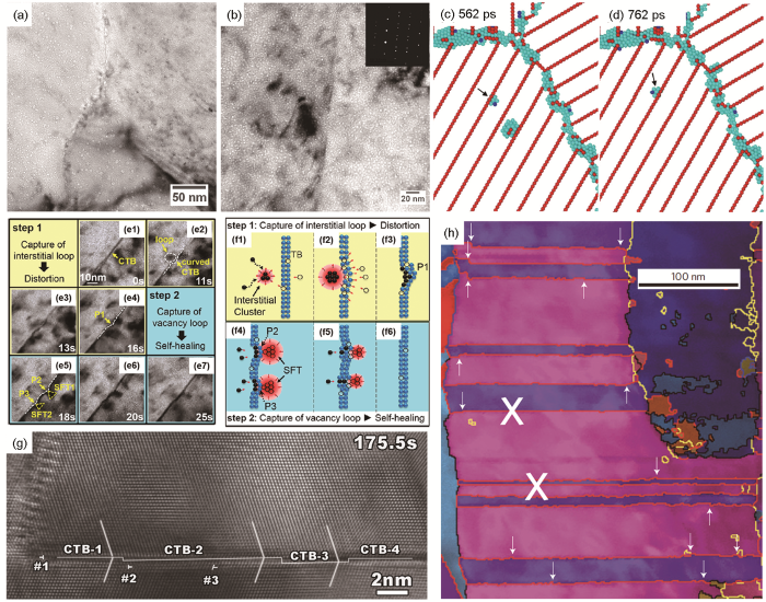
(a) cavity formation near the GB triple-junction[14](b) cavities near the twin boundary with its corresponding selected area electron diffraction (SAED) pattern[14](c, d) atomistic images showing a dumbbell crossing a CTB during equilibration after radiation cascade[28](e1-e7) in situ snapshots and schematics of distortion and self-healing of CTBs[26](f1-f6) schematics illustrate the capturing of defect clusters by CTBs and their self-healing mechanism(g) the interaction of lattice glide dislocation with a CTB, forming defective CTB[31]
(h) defective CTBs prevailing in deformed nanotwinned Cu structure. Some selected kinks are marked with white arrows. The portion of CTBs marked with an X is perfect TBs without defects[27]
Fig.1
Design of coherent twin boundary (CTB) and its response to the irradiation damage
Fig.2
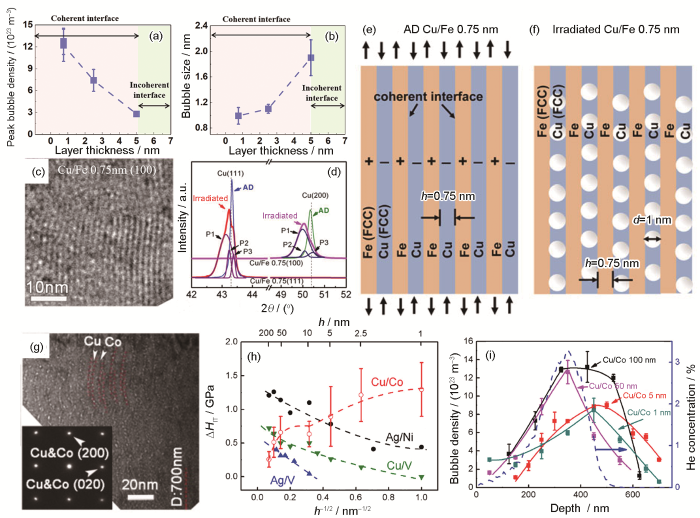
Design of coherent heterogeneous interfaces and their responses to the irradiation damage (a-f) the fully coherent fcc Cu/Fe nanolayers subjected to He ion irradiation[32] (a) the variation of peak He bubble density with layer thickness (h) (b) the variation of bubble size (d) with h (c) a cross-sectional TEM (XTEM) micrograph showing the layer interface retained and arrays of low-density He bubbles (with a diameter of ~1 nm or less) with an average separation distance of 1.5 nm were observed in the region close to the end of He concentration profile (d) XRD spectra of as-deposited (AD) and He ion irradiated Cu/Fe multilayers (e) prior to radiation of fully coherent immiscible Cu/Fe 0.75 nm multilayer, Cu is under compression and Fe is under tension (f) after radiation, He bubbles prefer to nucleate in Cu layers and are constricted to reside inside Cu layers (g, h) the fully coherent fcc Cu/Co nanolayers subjected to He ion irradiation[34] (g) XTEM showing clear alignment of He bubbles along layer interfaces. The embedded SAED pattern shows that the film retained epitaxial structure with fully coherent Cu/fcc Co stacking (h) inverse size-dependent radiation hardening in Cu/Co. The magnitude of radiation hardening is greater at smaller h (ΔHIT—indentation hardness) (i) comparison of the evolution of He bubble density along penetration depth in several Cu/Co multilayers[34]
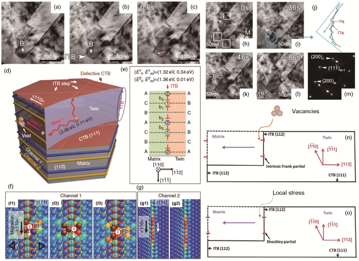
(a-c) in situ snapshots showing the migration and absorption of defect clusters by an ITB at the dose of about 0.85 dpa[37] (d-g) absorption and diffusion of interstitials in nanovoid-nanotwinned (nv-nt) Cu[38] (d) fast interstitial diffusion pipes enabled by incoherent twin boundary (ITB)-CTB networks in nanotwinned Cu (e) two fast diffusion channels at ITBs (Ef, Em—formation and migration energies, respectively) (f, g) the corresponding diffusion mechanisms (h-m) snapshots recorded during in situ irradiation in TEM and corresponding schematics showing the continuous evolution of twin boundaries over a dose range of 0.766-0.898 dpa[37] (n, o) schematics of ITB migration mechanisms during irradiation[37]
Fig.3
Design of incoherent twin boundary (ITB) and its response to the irradiation damage
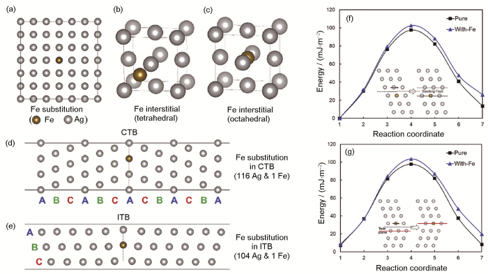
(a-e) configurations of Fe impurities in Ag at interstitial and substitutional sites at different locations used for DFT simulations
(f) creation of an intrinsic stacking fault in Ag with and without Fe substitutional atom (via shear displacement) showing the increase of the stable stacking fault energy by 12 mJ/m2, and the increase of unstable stacking fault energy by about 5 mJ/m2
(g) comparison of migration energy barrier for a coherent twin boundary with and without the Fe substitutional atom showing an increase of energy barrier by about 6 mJ/m2 with Fe substitutional atom at the original twin boundary
Fig.4
The density function theory (DFT) simulations results about the stability variation of the ITB after Fe addition[43]
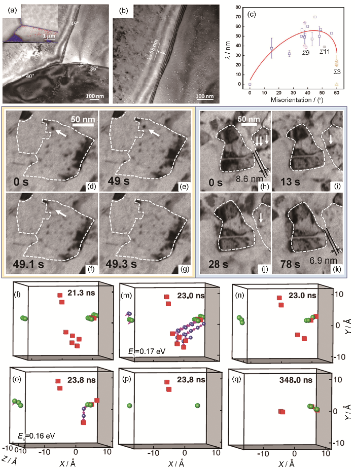
(a) defects near a triple junction in polycrystalline Cu irradiated at 450oC by 200 keV He ions with fluence of 2×10¹⁷ ions/cm2 (The inset is the corresponding electron backscatter diffraction (EBSD) image)[13]
(b) the determination of void-denuded zones (VDZ) for one grain boundary (GB) with 49°. All images were taken under a defocus of -5 μm[13] (λ—VDZ width)
(c) VDZ width as a function of misorientation for non-CTB ∑3 and ∑3 GBs[13] (d-k) in situ evidence of absorption of individual loops or a dislocation segment by GBs of nanocrystalline Ni[51] (l-q) selected snapshots of damage self-healing near the GB from temperature accelerated dynamics (TAD) simulations. The symbols are defined as follows: larger green spheres, interstitials; red cubes, vacancies; smaller blue spheres, atoms that move more than 1 nm during an event (between the frames immediately before and after); purple vectors, the moving directions and distances of moving atoms (Ea—activation barriers)[8] (l) after 21.3 ns, the five vacancies below the GB form a cluster (m, n) at 23.0 ns, three interstitials emit from the GB with a barrier of 0.17 eV to annihilate three vacancies. Note that Fig.5m shows how atoms move during this transition, and Fig.5n shows the final configuration after the event is completed (o, p) configurations before and after the last interstitial emission event at 23.8 ns (q) at 348.0 ns, the two vacancies above the GB diffuse to the GB via the slower conventional hopping mechanism
Fig.5
Design of high angle grain boundary and its interaction with the defects
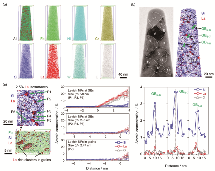
(b) a bright-field TEM image and corresponding APT Si atom map of a thin slice (5 nm in thickness) reconstructed volume, with 14 resolved nanograins marked as 1-14, respectively and GBs decorated with La-rich nanoprecipitates (NPs). 1D composition profiles across GB5–6, GB6–7, and GB7–8, as marked by green arrows in the Si map, showing the segregation of Si, La, and O at GBs
(c) a top magnified combined atom map of Si and La from a small reconstructed region with GBs decorated with La-rich NPs, a bottom combined Fe, Si, and La map of a small framed region of a grain containing a La-rich NP defined by iso-surfaces of 2.5%La (atomic fraction) and fine La-rich clusters. The right proxigrams from La-rich NPs in different sizes reveal their compositions of La-rich NPs at GBs and in grain interiors. The particle size (d) of NPs is defined as the equivalent spherical diameter
Fig.6
Correlative atom probe tomography (APT) and transmission electron microscopy (TEM) characterization of nanocrystalline austenitic stainless steel (NC-SS)[58](a) combined and individual element atom maps of the analyzed volume
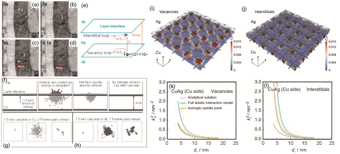
(a-d) in situ observation of dislocation loops absorbed by layer interface over a dose range of 0.131-0.133 dpa (0.262×10¹⁴-0.266×10¹⁴ ions/cm2)[10]
(e) schematic of interaction between two coaxial dislocation loops with opposite Burgers vectors[10] (f-h) simulations of 1.5 keV collision cascades in Cu/Nb multilayer composite (f), perfect crystalline fcc copper (g), and perfect crystalline bcc niobium (h)[63] (i, j) interface stress enhancing the sink strength of layer interfaces: Migration paths and local concentrations of vacancies (i) and interstitials (j) on the Ag side of the semi-coherent Ag-Cu interface[68] (k, l) enhancement in sink strength of semi-coherent Ag-Cu interfaces for vacancies (k) and interstitials (l) in Cu are plotted as functions of layer thickness ( and are the sink strengths for vacancies and interstitials, respectively, d1—layer thickness)[68]
Fig.7
Interaction between the semi-coherent interfaces and the irradiation-induced defects
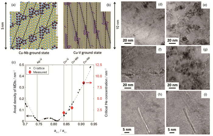
(a, b) the MDIs in Cu/Nb and Cu/V interfaces (The dashed lines indicate interface misfit dislocations)[74]
(c) the black dots present the areal densities of MDIs calculated by O-lattice theory for a range of fcc/bcc pairs with different lattice parameter ratios, but identical interface crystallography (Kurdjumov-Sachs orientation relation and closest-packed interface planes); the red diamonds are critical He concentrations measured to detect He bubbles in TEM; and the dashed line is a visual guide[74] (d-i) plan-view images of He channels[78] (d-g) underfocused plan-view TEM micrographs (400-nm underfocus) of the V/Cu/V trilayer after He implantation to fluences of 1×10¹⁵ ions/cm2 (d), 3×10¹⁵ ions/cm2 (e), 5×10¹⁵ ions/cm2 (f), and 1×10¹⁶ ions/cm2 (g) (h, i) an isolated precipitate from a sample implanted to 31015 ions/cm2 appears bright in underfocus (h) and dark in overfocus (i) imaging conditions (400-nm overfocus), confirming that it is an elongated, He filled cavity
Fig.8
Design of interfacial misfit intersections (MDIs) at the semi-coherent interfaces
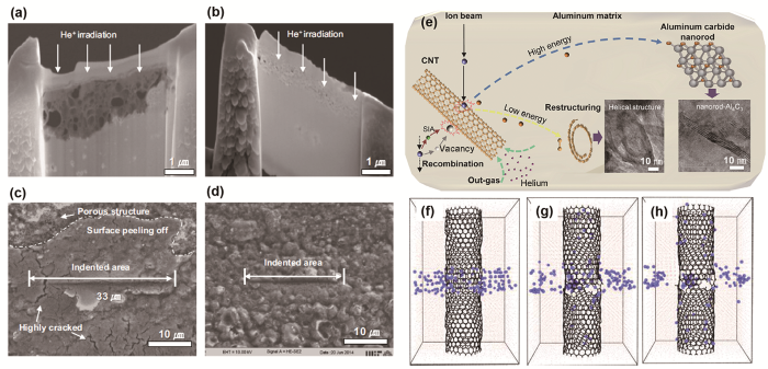
(a-d) SEM images of highly porous control Al (a) and Al+1%CNT (volume fraction) (b), and indented area observations on control Al (c) and Al+CNT composites (d)[79]
(e) schematic of shape changes on CNT, recombination, and helium out-gas[79] (f-h) molecular dynamics (MD) simulation snapshots (Ni: small red dots, C: small black spheres, He: blue spheres)[81] (f) at , when Ni/C atoms are replaced at random by He (g) evolution 0.05 ns later (h) 1.0 ns later. In Figs.9g and h, He atoms are diffusing along the interior and exterior walls of the CNT, far from the CNT center. When no CNT wall defects are included He atoms diffuse only along the CNT external wall
Fig.9
Irradiation responses of the carbon nanotube (CNT)/metal interfaces
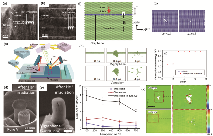
(a) TEM image of as-deposited W nanofilm irradiated by 50 keV He+ ions to a total influence of 1×10¹⁷ ions/cm2 [82]
(b) TEM image of peak He concentration region under 50 keV He+ irradiation in W15/Gr to a total influence of 5×10¹⁶ ions/cm2[82]
(c) schematic of the experimental setup for characterizing the thermal resistance[82] (d, e) SEM images of nanopillars after compression testing for He+ irradiated pure V (d) and V-graphene with 110 nm repeat layer spacing indicating that the crack propagation was suppressed by the graphene interface (e)[83] (f) schematic of simulation[83] (g) damage on graphene after the knock-on event[83] (h) the collision cascade after the knock-on event for d=1.5 nm. The amount of cascade is significantly reduced by the graphene layer. Significantly more defects remain in the pure V. Atoms with high potential energy (above -4.4 eV) are visualized selectively[83] (i) the formation energies of vacancies are significantly lower at the graphene interface than that in the bulk lattice of V[83] (j) number of surviving defects in the bulk region, generated by a 3 keV primary knock-on atom (PKA) away from the interface about 1.54 nm, as a function of temperature[84] (k) effects of the displacement cascades generated by a 100 keV PKA on the different layers of graphene of Gr/Cu nanolayered composites, viewed in the z-direction[84]
Fig.10
Irradiation responses of the graphene (Gr)/metal interfaces
(a) defects near a triple junction in polycrystalline Cu irradiated at 450oC by 200 keV He ions with fluence of 2×10¹⁷ ions/cm2 (The inset is the corresponding electron backscatter diffraction (EBSD) image)[13] ...
... (c) VDZ width as a function of misorientation for non-CTB ∑3 and ∑3 GBs[13] (d-k) in situ evidence of absorption of individual loops or a dislocation segment by GBs of nanocrystalline Ni[51] (l-q) selected snapshots of damage self-healing near the GB from temperature accelerated dynamics (TAD) simulations. The symbols are defined as follows: larger green spheres, interstitials; red cubes, vacancies; smaller blue spheres, atoms that move more than 1 nm during an event (between the frames immediately before and after); purple vectors, the moving directions and distances of moving atoms (Ea—activation barriers)[8] (l) after 21.3 ns, the five vacancies below the GB form a cluster (m, n) at 23.0 ns, three interstitials emit from the GB with a barrier of 0.17 eV to annihilate three vacancies. Note that Fig.5m shows how atoms move during this transition, and Fig.5n shows the final configuration after the event is completed (o, p) configurations before and after the last interstitial emission event at 23.8 ns (q) at 348.0 ns, the two vacancies above the GB diffuse to the GB via the slower conventional hopping mechanism ...
(a-d) in situ observation of dislocation loops absorbed by layer interface over a dose range of 0.131-0.133 dpa (0.262×10¹⁴-0.266×10¹⁴ ions/cm2)[10] ...
... (a-d) in situ observation of dislocation loops absorbed by layer interface over a dose range of 0.131-0.133 dpa (0.262×10¹⁴-0.266×10¹⁴ ions/cm2)[10] ...
... (e) schematic of interaction between two coaxial dislocation loops with opposite Burgers vectors[10] (f-h) simulations of 1.5 keV collision cascades in Cu/Nb multilayer composite (f), perfect crystalline fcc copper (g), and perfect crystalline bcc niobium (h)[63] (i, j) interface stress enhancing the sink strength of layer interfaces: Migration paths and local concentrations of vacancies (i) and interstitials (j) on the Ag side of the semi-coherent Ag-Cu interface[68] (k, l) enhancement in sink strength of semi-coherent Ag-Cu interfaces for vacancies (k) and interstitials (l) in Cu are plotted as functions of layer thickness ( and are the sink strengths for vacancies and interstitials, respectively, d1—layer thickness)[68] ...
Design of radiation tolerant materials via interface engineering
(a) defects near a triple junction in polycrystalline Cu irradiated at 450oC by 200 keV He ions with fluence of 2×10¹⁷ ions/cm2 (The inset is the corresponding electron backscatter diffraction (EBSD) image)[13] ...
... (a) defects near a triple junction in polycrystalline Cu irradiated at 450oC by 200 keV He ions with fluence of 2×10¹⁷ ions/cm2 (The inset is the corresponding electron backscatter diffraction (EBSD) image)[13] ...
... (b) the determination of void-denuded zones (VDZ) for one grain boundary (GB) with 49°. All images were taken under a defocus of -5 μm[13] (λ—VDZ width) ...
... (c) VDZ width as a function of misorientation for non-CTB ∑3 and ∑3 GBs[13] (d-k) in situ evidence of absorption of individual loops or a dislocation segment by GBs of nanocrystalline Ni[51] (l-q) selected snapshots of damage self-healing near the GB from temperature accelerated dynamics (TAD) simulations. The symbols are defined as follows: larger green spheres, interstitials; red cubes, vacancies; smaller blue spheres, atoms that move more than 1 nm during an event (between the frames immediately before and after); purple vectors, the moving directions and distances of moving atoms (Ea—activation barriers)[8] (l) after 21.3 ns, the five vacancies below the GB form a cluster (m, n) at 23.0 ns, three interstitials emit from the GB with a barrier of 0.17 eV to annihilate three vacancies. Note that Fig.5m shows how atoms move during this transition, and Fig.5n shows the final configuration after the event is completed (o, p) configurations before and after the last interstitial emission event at 23.8 ns (q) at 348.0 ns, the two vacancies above the GB diffuse to the GB via the slower conventional hopping mechanism ...
(a) cavity formation near the GB triple-junction[14](b) cavities near the twin boundary with its corresponding selected area electron diffraction (SAED) pattern[14](c, d) atomistic images showing a dumbbell crossing a CTB during equilibration after radiation cascade[28](e1-e7) in situ snapshots and schematics of distortion and self-healing of CTBs[26](f1-f6) schematics illustrate the capturing of defect clusters by CTBs and their self-healing mechanism(g) the interaction of lattice glide dislocation with a CTB, forming defective CTB[31] ...
... (a) cavity formation near the GB triple-junction[14](b) cavities near the twin boundary with its corresponding selected area electron diffraction (SAED) pattern[14](c, d) atomistic images showing a dumbbell crossing a CTB during equilibration after radiation cascade[28](e1-e7) in situ snapshots and schematics of distortion and self-healing of CTBs[26](f1-f6) schematics illustrate the capturing of defect clusters by CTBs and their self-healing mechanism(g) the interaction of lattice glide dislocation with a CTB, forming defective CTB[31] ...
... [14](c, d) atomistic images showing a dumbbell crossing a CTB during equilibration after radiation cascade[28](e1-e7) in situ snapshots and schematics of distortion and self-healing of CTBs[26](f1-f6) schematics illustrate the capturing of defect clusters by CTBs and their self-healing mechanism(g) the interaction of lattice glide dislocation with a CTB, forming defective CTB[31] ...
Quantitative comparison of sink efficiency of Cu-Nb, Cu-V and Cu-Ni interfaces for point defects
(a) cavity formation near the GB triple-junction[14](b) cavities near the twin boundary with its corresponding selected area electron diffraction (SAED) pattern[14](c, d) atomistic images showing a dumbbell crossing a CTB during equilibration after radiation cascade[28](e1-e7) in situ snapshots and schematics of distortion and self-healing of CTBs[26](f1-f6) schematics illustrate the capturing of defect clusters by CTBs and their self-healing mechanism(g) the interaction of lattice glide dislocation with a CTB, forming defective CTB[31] ...
... (a) cavity formation near the GB triple-junction[14](b) cavities near the twin boundary with its corresponding selected area electron diffraction (SAED) pattern[14](c, d) atomistic images showing a dumbbell crossing a CTB during equilibration after radiation cascade[28](e1-e7) in situ snapshots and schematics of distortion and self-healing of CTBs[26](f1-f6) schematics illustrate the capturing of defect clusters by CTBs and their self-healing mechanism(g) the interaction of lattice glide dislocation with a CTB, forming defective CTB[31] ...
... (h) defective CTBs prevailing in deformed nanotwinned Cu structure. Some selected kinks are marked with white arrows. The portion of CTBs marked with an X is perfect TBs without defects[27] ...
(a) cavity formation near the GB triple-junction[14](b) cavities near the twin boundary with its corresponding selected area electron diffraction (SAED) pattern[14](c, d) atomistic images showing a dumbbell crossing a CTB during equilibration after radiation cascade[28](e1-e7) in situ snapshots and schematics of distortion and self-healing of CTBs[26](f1-f6) schematics illustrate the capturing of defect clusters by CTBs and their self-healing mechanism(g) the interaction of lattice glide dislocation with a CTB, forming defective CTB[31] ...
... (a) cavity formation near the GB triple-junction[14](b) cavities near the twin boundary with its corresponding selected area electron diffraction (SAED) pattern[14](c, d) atomistic images showing a dumbbell crossing a CTB during equilibration after radiation cascade[28](e1-e7) in situ snapshots and schematics of distortion and self-healing of CTBs[26](f1-f6) schematics illustrate the capturing of defect clusters by CTBs and their self-healing mechanism(g) the interaction of lattice glide dislocation with a CTB, forming defective CTB[31] ...
Interactions between non-screw lattice dislocations and coherent twin boundaries in face-centered cubic metals
(a) cavity formation near the GB triple-junction[14](b) cavities near the twin boundary with its corresponding selected area electron diffraction (SAED) pattern[14](c, d) atomistic images showing a dumbbell crossing a CTB during equilibration after radiation cascade[28](e1-e7) in situ snapshots and schematics of distortion and self-healing of CTBs[26](f1-f6) schematics illustrate the capturing of defect clusters by CTBs and their self-healing mechanism(g) the interaction of lattice glide dislocation with a CTB, forming defective CTB[31] ...
... (a) cavity formation near the GB triple-junction[14](b) cavities near the twin boundary with its corresponding selected area electron diffraction (SAED) pattern[14](c, d) atomistic images showing a dumbbell crossing a CTB during equilibration after radiation cascade[28](e1-e7) in situ snapshots and schematics of distortion and self-healing of CTBs[26](f1-f6) schematics illustrate the capturing of defect clusters by CTBs and their self-healing mechanism(g) the interaction of lattice glide dislocation with a CTB, forming defective CTB[31] ...
... [32,34]Design of coherent heterogeneous interfaces and their responses to the irradiation damage (a-f) the fully coherent fcc Cu/Fe nanolayers subjected to He ion irradiation<sup>[<xref ref-type="bibr" rid="R32">32</xref>]</sup> (a) the variation of peak He bubble density with layer thickness (<i>h</i>) (b) the variation of bubble size (<i>d</i>) with<i> h</i> (c) a cross-sectional TEM (XTEM) micrograph showing the layer interface retained and arrays of low-density He bubbles (with a diameter of ~1 nm or less) with an average separation distance of 1.5 nm were observed in the region close to the end of He concentration profile (d) XRD spectra of as-deposited (AD) and He ion irradiated Cu/Fe multilayers (e) prior to radiation of fully coherent immiscible Cu/Fe 0.75 nm multilayer, Cu is under compression and Fe is under tension (f) after radiation, He bubbles prefer to nucleate in Cu layers and are constricted to reside inside Cu layers (g, h) the fully coherent fcc Cu/Co nanolayers subjected to He ion irradiation<sup>[<xref ref-type="bibr" rid="R34">34</xref>]</sup> (g) XTEM showing clear alignment of He bubbles along layer interfaces. The embedded SAED pattern shows that the film retained epitaxial structure with fully coherent Cu/fcc Co stacking (h) inverse size-dependent radiation hardening in Cu/Co. The magnitude of radiation hardening is greater at smaller <i>h </i>(Δ<i>H</i><sub>IT</sub>—indentation hardness) (i) comparison of the evolution of He bubble density along penetration depth in several Cu/Co multilayers<sup>[<xref ref-type="bibr" rid="R34">34</xref>]</sup>Fig.2
... [32] (a) the variation of peak He bubble density with layer thickness (h) (b) the variation of bubble size (d) with h (c) a cross-sectional TEM (XTEM) micrograph showing the layer interface retained and arrays of low-density He bubbles (with a diameter of ~1 nm or less) with an average separation distance of 1.5 nm were observed in the region close to the end of He concentration profile (d) XRD spectra of as-deposited (AD) and He ion irradiated Cu/Fe multilayers (e) prior to radiation of fully coherent immiscible Cu/Fe 0.75 nm multilayer, Cu is under compression and Fe is under tension (f) after radiation, He bubbles prefer to nucleate in Cu layers and are constricted to reside inside Cu layers (g, h) the fully coherent fcc Cu/Co nanolayers subjected to He ion irradiation[34] (g) XTEM showing clear alignment of He bubbles along layer interfaces. The embedded SAED pattern shows that the film retained epitaxial structure with fully coherent Cu/fcc Co stacking (h) inverse size-dependent radiation hardening in Cu/Co. The magnitude of radiation hardening is greater at smaller h (ΔHIT—indentation hardness) (i) comparison of the evolution of He bubble density along penetration depth in several Cu/Co multilayers[34]Fig.2
Design of coherent heterogeneous interfaces and their responses to the irradiation damage (a-f) the fully coherent fcc Cu/Fe nanolayers subjected to He ion irradiation<sup>[<xref ref-type="bibr" rid="R32">32</xref>]</sup> (a) the variation of peak He bubble density with layer thickness (<i>h</i>) (b) the variation of bubble size (<i>d</i>) with<i> h</i> (c) a cross-sectional TEM (XTEM) micrograph showing the layer interface retained and arrays of low-density He bubbles (with a diameter of ~1 nm or less) with an average separation distance of 1.5 nm were observed in the region close to the end of He concentration profile (d) XRD spectra of as-deposited (AD) and He ion irradiated Cu/Fe multilayers (e) prior to radiation of fully coherent immiscible Cu/Fe 0.75 nm multilayer, Cu is under compression and Fe is under tension (f) after radiation, He bubbles prefer to nucleate in Cu layers and are constricted to reside inside Cu layers (g, h) the fully coherent fcc Cu/Co nanolayers subjected to He ion irradiation<sup>[<xref ref-type="bibr" rid="R34">34</xref>]</sup> (g) XTEM showing clear alignment of He bubbles along layer interfaces. The embedded SAED pattern shows that the film retained epitaxial structure with fully coherent Cu/fcc Co stacking (h) inverse size-dependent radiation hardening in Cu/Co. The magnitude of radiation hardening is greater at smaller <i>h </i>(Δ<i>H</i><sub>IT</sub>—indentation hardness) (i) comparison of the evolution of He bubble density along penetration depth in several Cu/Co multilayers<sup>[<xref ref-type="bibr" rid="R34">34</xref>]</sup>Fig.2
... [34] (g) XTEM showing clear alignment of He bubbles along layer interfaces. The embedded SAED pattern shows that the film retained epitaxial structure with fully coherent Cu/fcc Co stacking (h) inverse size-dependent radiation hardening in Cu/Co. The magnitude of radiation hardening is greater at smaller h (ΔHIT—indentation hardness) (i) comparison of the evolution of He bubble density along penetration depth in several Cu/Co multilayers[34]Fig.2
(a-c) in situ snapshots showing the migration and absorption of defect clusters by an ITB at the dose of about 0.85 dpa[37] (d-g) absorption and diffusion of interstitials in nanovoid-nanotwinned (nv-nt) Cu[38] (d) fast interstitial diffusion pipes enabled by incoherent twin boundary (ITB)-CTB networks in nanotwinned Cu (e) two fast diffusion channels at ITBs (Ef, Em—formation and migration energies, respectively) (f, g) the corresponding diffusion mechanisms (h-m) snapshots recorded during in situ irradiation in TEM and corresponding schematics showing the continuous evolution of twin boundaries over a dose range of 0.766-0.898 dpa[37] (n, o) schematics of ITB migration mechanisms during irradiation[37] ...
... (a-c) in situ snapshots showing the migration and absorption of defect clusters by an ITB at the dose of about 0.85 dpa[37] (d-g) absorption and diffusion of interstitials in nanovoid-nanotwinned (nv-nt) Cu[38] (d) fast interstitial diffusion pipes enabled by incoherent twin boundary (ITB)-CTB networks in nanotwinned Cu (e) two fast diffusion channels at ITBs (Ef, Em—formation and migration energies, respectively) (f, g) the corresponding diffusion mechanisms (h-m) snapshots recorded during in situ irradiation in TEM and corresponding schematics showing the continuous evolution of twin boundaries over a dose range of 0.766-0.898 dpa[37] (n, o) schematics of ITB migration mechanisms during irradiation[37] ...
... [37] (n, o) schematics of ITB migration mechanisms during irradiation[37] ...
(a-c) in situ snapshots showing the migration and absorption of defect clusters by an ITB at the dose of about 0.85 dpa[37] (d-g) absorption and diffusion of interstitials in nanovoid-nanotwinned (nv-nt) Cu[38] (d) fast interstitial diffusion pipes enabled by incoherent twin boundary (ITB)-CTB networks in nanotwinned Cu (e) two fast diffusion channels at ITBs (Ef, Em—formation and migration energies, respectively) (f, g) the corresponding diffusion mechanisms (h-m) snapshots recorded during in situ irradiation in TEM and corresponding schematics showing the continuous evolution of twin boundaries over a dose range of 0.766-0.898 dpa[37] (n, o) schematics of ITB migration mechanisms during irradiation[37] ...
... (a-c) in situ snapshots showing the migration and absorption of defect clusters by an ITB at the dose of about 0.85 dpa[37] (d-g) absorption and diffusion of interstitials in nanovoid-nanotwinned (nv-nt) Cu[38] (d) fast interstitial diffusion pipes enabled by incoherent twin boundary (ITB)-CTB networks in nanotwinned Cu (e) two fast diffusion channels at ITBs (Ef, Em—formation and migration energies, respectively) (f, g) the corresponding diffusion mechanisms (h-m) snapshots recorded during in situ irradiation in TEM and corresponding schematics showing the continuous evolution of twin boundaries over a dose range of 0.766-0.898 dpa[37] (n, o) schematics of ITB migration mechanisms during irradiation[37] ...
Incoherent twin boundary migration induced by ion irradiation in Cu
(a-e) configurations of Fe impurities in Ag at interstitial and substitutional sites at different locations used for DFT simulations ...
... (g) comparison of migration energy barrier for a coherent twin boundary with and without the Fe substitutional atom showing an increase of energy barrier by about 6 mJ/m2 with Fe substitutional atom at the original twin boundaryThe density function theory (DFT) simulations results about the stability variation of the ITB after Fe addition<sup>[<xref ref-type="bibr" rid="R43">43</xref>]</sup>Fig.4<strong>2.2 </strong>大角度晶界辐照行为研究
(a) defects near a triple junction in polycrystalline Cu irradiated at 450oC by 200 keV He ions with fluence of 2×10¹⁷ ions/cm2 (The inset is the corresponding electron backscatter diffraction (EBSD) image)[13] ...
... (c) VDZ width as a function of misorientation for non-CTB ∑3 and ∑3 GBs[13] (d-k) in situ evidence of absorption of individual loops or a dislocation segment by GBs of nanocrystalline Ni[51] (l-q) selected snapshots of damage self-healing near the GB from temperature accelerated dynamics (TAD) simulations. The symbols are defined as follows: larger green spheres, interstitials; red cubes, vacancies; smaller blue spheres, atoms that move more than 1 nm during an event (between the frames immediately before and after); purple vectors, the moving directions and distances of moving atoms (Ea—activation barriers)[8] (l) after 21.3 ns, the five vacancies below the GB form a cluster (m, n) at 23.0 ns, three interstitials emit from the GB with a barrier of 0.17 eV to annihilate three vacancies. Note that Fig.5m shows how atoms move during this transition, and Fig.5n shows the final configuration after the event is completed (o, p) configurations before and after the last interstitial emission event at 23.8 ns (q) at 348.0 ns, the two vacancies above the GB diffuse to the GB via the slower conventional hopping mechanism ...
(b) a bright-field TEM image and corresponding APT Si atom map of a thin slice (5 nm in thickness) reconstructed volume, with 14 resolved nanograins marked as 1-14, respectively and GBs decorated with La-rich nanoprecipitates (NPs). 1D composition profiles across GB5–6, GB6–7, and GB7–8, as marked by green arrows in the Si map, showing the segregation of Si, La, and O at GBs ...
... (c) a top magnified combined atom map of Si and La from a small reconstructed region with GBs decorated with La-rich NPs, a bottom combined Fe, Si, and La map of a small framed region of a grain containing a La-rich NP defined by iso-surfaces of 2.5%La (atomic fraction) and fine La-rich clusters. The right proxigrams from La-rich NPs in different sizes reveal their compositions of La-rich NPs at GBs and in grain interiors. The particle size (d) of NPs is defined as the equivalent spherical diameterCorrelative atom probe tomography (APT) and transmission electron microscopy (TEM) characterization of nanocrystalline austenitic stainless steel (NC-SS)<sup>[<xref ref-type="bibr" rid="R58">58</xref>]</sup>(a) combined and individual element atom maps of the analyzed volumeFig.6
(a-d) in situ observation of dislocation loops absorbed by layer interface over a dose range of 0.131-0.133 dpa (0.262×10¹⁴-0.266×10¹⁴ ions/cm2)[10] ...
... (e) schematic of interaction between two coaxial dislocation loops with opposite Burgers vectors[10] (f-h) simulations of 1.5 keV collision cascades in Cu/Nb multilayer composite (f), perfect crystalline fcc copper (g), and perfect crystalline bcc niobium (h)[63] (i, j) interface stress enhancing the sink strength of layer interfaces: Migration paths and local concentrations of vacancies (i) and interstitials (j) on the Ag side of the semi-coherent Ag-Cu interface[68] (k, l) enhancement in sink strength of semi-coherent Ag-Cu interfaces for vacancies (k) and interstitials (l) in Cu are plotted as functions of layer thickness ( and are the sink strengths for vacancies and interstitials, respectively, d1—layer thickness)[68] ...
Interface structure and radiation damage resistance in Cu-Nb multilayer nanocomposites
(a-d) in situ observation of dislocation loops absorbed by layer interface over a dose range of 0.131-0.133 dpa (0.262×10¹⁴-0.266×10¹⁴ ions/cm2)[10] ...
... (e) schematic of interaction between two coaxial dislocation loops with opposite Burgers vectors[10] (f-h) simulations of 1.5 keV collision cascades in Cu/Nb multilayer composite (f), perfect crystalline fcc copper (g), and perfect crystalline bcc niobium (h)[63] (i, j) interface stress enhancing the sink strength of layer interfaces: Migration paths and local concentrations of vacancies (i) and interstitials (j) on the Ag side of the semi-coherent Ag-Cu interface[68] (k, l) enhancement in sink strength of semi-coherent Ag-Cu interfaces for vacancies (k) and interstitials (l) in Cu are plotted as functions of layer thickness ( and are the sink strengths for vacancies and interstitials, respectively, d1—layer thickness)[68] ...
... [68] ...
A review of recent theoretical developments in the understanding of the migration of helium in metals and its interaction with lattice defects
(a, b) the MDIs in Cu/Nb and Cu/V interfaces (The dashed lines indicate interface misfit dislocations)[74] ...
... (a, b) the MDIs in Cu/Nb and Cu/V interfaces (The dashed lines indicate interface misfit dislocations)[74] ...
... (c) the black dots present the areal densities of MDIs calculated by O-lattice theory for a range of fcc/bcc pairs with different lattice parameter ratios, but identical interface crystallography (Kurdjumov-Sachs orientation relation and closest-packed interface planes); the red diamonds are critical He concentrations measured to detect He bubbles in TEM; and the dashed line is a visual guide[74] (d-i) plan-view images of He channels[78] (d-g) underfocused plan-view TEM micrographs (400-nm underfocus) of the V/Cu/V trilayer after He implantation to fluences of 1×10¹⁵ ions/cm2 (d), 3×10¹⁵ ions/cm2 (e), 5×10¹⁵ ions/cm2 (f), and 1×10¹⁶ ions/cm2 (g) (h, i) an isolated precipitate from a sample implanted to 31015 ions/cm2 appears bright in underfocus (h) and dark in overfocus (i) imaging conditions (400-nm overfocus), confirming that it is an elongated, He filled cavity ...
O-lattice calculation of an F.C.C.-B.C.C. interface
(a, b) the MDIs in Cu/Nb and Cu/V interfaces (The dashed lines indicate interface misfit dislocations)[74] ...
... (c) the black dots present the areal densities of MDIs calculated by O-lattice theory for a range of fcc/bcc pairs with different lattice parameter ratios, but identical interface crystallography (Kurdjumov-Sachs orientation relation and closest-packed interface planes); the red diamonds are critical He concentrations measured to detect He bubbles in TEM; and the dashed line is a visual guide[74] (d-i) plan-view images of He channels[78] (d-g) underfocused plan-view TEM micrographs (400-nm underfocus) of the V/Cu/V trilayer after He implantation to fluences of 1×10¹⁵ ions/cm2 (d), 3×10¹⁵ ions/cm2 (e), 5×10¹⁵ ions/cm2 (f), and 1×10¹⁶ ions/cm2 (g) (h, i) an isolated precipitate from a sample implanted to 31015 ions/cm2 appears bright in underfocus (h) and dark in overfocus (i) imaging conditions (400-nm overfocus), confirming that it is an elongated, He filled cavity ...
Dispersion of carbon nanotubes in aluminum improves radiation resistance
(a-d) SEM images of highly porous control Al (a) and Al+1%CNT (volume fraction) (b), and indented area observations on control Al (c) and Al+CNT composites (d)[79] ...
... (a-d) SEM images of highly porous control Al (a) and Al+1%CNT (volume fraction) (b), and indented area observations on control Al (c) and Al+CNT composites (d)[79] ...
... (e) schematic of shape changes on CNT, recombination, and helium out-gas[79] (f-h) molecular dynamics (MD) simulation snapshots (Ni: small red dots, C: small black spheres, He: blue spheres)[81] (f) at , when Ni/C atoms are replaced at random by He (g) evolution 0.05 ns later (h) 1.0 ns later. In Figs.9g and h, He atoms are diffusing along the interior and exterior walls of the CNT, far from the CNT center. When no CNT wall defects are included He atoms diffuse only along the CNT external wall ...
(a-d) SEM images of highly porous control Al (a) and Al+1%CNT (volume fraction) (b), and indented area observations on control Al (c) and Al+CNT composites (d)[79] ...
... (e) schematic of shape changes on CNT, recombination, and helium out-gas[79] (f-h) molecular dynamics (MD) simulation snapshots (Ni: small red dots, C: small black spheres, He: blue spheres)[81] (f) at , when Ni/C atoms are replaced at random by He (g) evolution 0.05 ns later (h) 1.0 ns later. In Figs.9g and h, He atoms are diffusing along the interior and exterior walls of the CNT, far from the CNT center. When no CNT wall defects are included He atoms diffuse only along the CNT external wall ...
Significant radiation tolerance and moderate reduction in thermal transport of a tungsten nanofilm by inserting monolayer graphene
(a) TEM image of as-deposited W nanofilm irradiated by 50 keV He+ ions to a total influence of 1×10¹⁷ ions/cm2 [82] ...
... (a) TEM image of as-deposited W nanofilm irradiated by 50 keV He+ ions to a total influence of 1×10¹⁷ ions/cm2 [82] ...
... (b) TEM image of peak He concentration region under 50 keV He+ irradiation in W15/Gr to a total influence of 5×10¹⁶ ions/cm2[82] ...
... (c) schematic of the experimental setup for characterizing the thermal resistance[82] (d, e) SEM images of nanopillars after compression testing for He+ irradiated pure V (d) and V-graphene with 110 nm repeat layer spacing indicating that the crack propagation was suppressed by the graphene interface (e)[83] (f) schematic of simulation[83] (g) damage on graphene after the knock-on event[83] (h) the collision cascade after the knock-on event for d=1.5 nm. The amount of cascade is significantly reduced by the graphene layer. Significantly more defects remain in the pure V. Atoms with high potential energy (above -4.4 eV) are visualized selectively[83] (i) the formation energies of vacancies are significantly lower at the graphene interface than that in the bulk lattice of V[83] (j) number of surviving defects in the bulk region, generated by a 3 keV primary knock-on atom (PKA) away from the interface about 1.54 nm, as a function of temperature[84] (k) effects of the displacement cascades generated by a 100 keV PKA on the different layers of graphene of Gr/Cu nanolayered composites, viewed in the z-direction[84] ...
... (c) schematic of the experimental setup for characterizing the thermal resistance[82] (d, e) SEM images of nanopillars after compression testing for He+ irradiated pure V (d) and V-graphene with 110 nm repeat layer spacing indicating that the crack propagation was suppressed by the graphene interface (e)[83] (f) schematic of simulation[83] (g) damage on graphene after the knock-on event[83] (h) the collision cascade after the knock-on event for d=1.5 nm. The amount of cascade is significantly reduced by the graphene layer. Significantly more defects remain in the pure V. Atoms with high potential energy (above -4.4 eV) are visualized selectively[83] (i) the formation energies of vacancies are significantly lower at the graphene interface than that in the bulk lattice of V[83] (j) number of surviving defects in the bulk region, generated by a 3 keV primary knock-on atom (PKA) away from the interface about 1.54 nm, as a function of temperature[84] (k) effects of the displacement cascades generated by a 100 keV PKA on the different layers of graphene of Gr/Cu nanolayered composites, viewed in the z-direction[84] ...
... [83] (g) damage on graphene after the knock-on event[83] (h) the collision cascade after the knock-on event for d=1.5 nm. The amount of cascade is significantly reduced by the graphene layer. Significantly more defects remain in the pure V. Atoms with high potential energy (above -4.4 eV) are visualized selectively[83] (i) the formation energies of vacancies are significantly lower at the graphene interface than that in the bulk lattice of V[83] (j) number of surviving defects in the bulk region, generated by a 3 keV primary knock-on atom (PKA) away from the interface about 1.54 nm, as a function of temperature[84] (k) effects of the displacement cascades generated by a 100 keV PKA on the different layers of graphene of Gr/Cu nanolayered composites, viewed in the z-direction[84] ...
... [83] (h) the collision cascade after the knock-on event for d=1.5 nm. The amount of cascade is significantly reduced by the graphene layer. Significantly more defects remain in the pure V. Atoms with high potential energy (above -4.4 eV) are visualized selectively[83] (i) the formation energies of vacancies are significantly lower at the graphene interface than that in the bulk lattice of V[83] (j) number of surviving defects in the bulk region, generated by a 3 keV primary knock-on atom (PKA) away from the interface about 1.54 nm, as a function of temperature[84] (k) effects of the displacement cascades generated by a 100 keV PKA on the different layers of graphene of Gr/Cu nanolayered composites, viewed in the z-direction[84] ...
... [83] (i) the formation energies of vacancies are significantly lower at the graphene interface than that in the bulk lattice of V[83] (j) number of surviving defects in the bulk region, generated by a 3 keV primary knock-on atom (PKA) away from the interface about 1.54 nm, as a function of temperature[84] (k) effects of the displacement cascades generated by a 100 keV PKA on the different layers of graphene of Gr/Cu nanolayered composites, viewed in the z-direction[84] ...
... [83] (j) number of surviving defects in the bulk region, generated by a 3 keV primary knock-on atom (PKA) away from the interface about 1.54 nm, as a function of temperature[84] (k) effects of the displacement cascades generated by a 100 keV PKA on the different layers of graphene of Gr/Cu nanolayered composites, viewed in the z-direction[84] ...
(a) TEM image of as-deposited W nanofilm irradiated by 50 keV He+ ions to a total influence of 1×10¹⁷ ions/cm2 [82] ...
... (c) schematic of the experimental setup for characterizing the thermal resistance[82] (d, e) SEM images of nanopillars after compression testing for He+ irradiated pure V (d) and V-graphene with 110 nm repeat layer spacing indicating that the crack propagation was suppressed by the graphene interface (e)[83] (f) schematic of simulation[83] (g) damage on graphene after the knock-on event[83] (h) the collision cascade after the knock-on event for d=1.5 nm. The amount of cascade is significantly reduced by the graphene layer. Significantly more defects remain in the pure V. Atoms with high potential energy (above -4.4 eV) are visualized selectively[83] (i) the formation energies of vacancies are significantly lower at the graphene interface than that in the bulk lattice of V[83] (j) number of surviving defects in the bulk region, generated by a 3 keV primary knock-on atom (PKA) away from the interface about 1.54 nm, as a function of temperature[84] (k) effects of the displacement cascades generated by a 100 keV PKA on the different layers of graphene of Gr/Cu nanolayered composites, viewed in the z-direction[84] ...


