


电镀Cu得益于其成本低、导电性好被广泛用于铜柱凸点(copper pillar,CuP)、再分布线(redistribution layer,RDL)和硅通孔(through silicon via,TSV)等集成电路先进封装结构中。近年来,3D封装以及器件小型化的趋势对先进封装中电镀Cu材料理化性能也提出了更加严苛的要求[1,2]。Cu直接暴露在空气中容易氧化是先进封装过程中需要解决的问题。关于Cu氧化机理的研究以及如何提升其抗氧化性能已经被广泛研究。李薰和骆继勋[3]研究了温度对于Cu氧化行为的影响。Kusano等[4]认为,影响氧化速率的关键因素是氧化物厚度而不是氧化温度,并且在40~160℃条件下所有单晶Cu呈现出相同的氧化物层生长趋势。Young等[5]提出,在70~178℃条件下,Cu的氧化速率取决于晶体取向。(111)取向纳米孪晶Cu (下文简称(111)nt-Cu)作为潜在的一般随机取向多晶组织Cu (下文简称C-Cu)的替代品,有着诸多优于C-Cu的性质。例如,更高的导电性、更好的抗电迁移性以及更加优异的力学性能[6~11]。
凸点下金属化层(under-bump metallization,UBM)作为先进倒装封装中的关键工艺之一,连接着焊料凸点与芯片或再分布线焊盘,其质量直接影响焊点质量、封装的成功率和封装后焊点的可靠性。在Cu-Cu直接键合领域,(111)nt-Cu也有其优势[12~18]。Juang等[12]在450~100℃和非真空环境中,用5 min的时间实现了(111)nt-Cu的直接键合。Liu等[13]在0.69 MPa和200℃的条件下,用不到60 min的时间实现了(111)nt-Cu的直接键合。在相对短的时间、低的温度和压力以及相对不严苛的气氛条件下,(111)nt-Cu可以实现Cu-Cu键合的要求。这得益于在150~300℃的温度区间内,Cu原子在(111)晶面上快速扩散的能力[14,15]。此外,在焊料的界面反应方面,(111)nt-Cu的优势也在近些年陆续被挖掘出来。Lin等[15]发现,在Sn/(111)nt-Cu界面,Cu6Sn5金属间化合物的晶体有强(001)取向。此外,在170℃热时效过程中,(111)nt-Cu基板对于Sn/(111)nt-Cu焊点有促进其界面Kirkendall孔洞自愈合的作用[16]。
1 实验方法
1.1 电沉积法制备Cu基板
采用直流电沉积法制备2种Cu基体,不同的组织采用的电镀液不同。其中C-Cu电镀液来自于商用产品(120~200 g/L CuSO4·5H2O,3~80 mL/L H2SO4,30~100 mg/L NaCl),而(111)nt-Cu电镀液为自行研制[30]。采用带有(111)择优取向的Cu种子层的晶圆作为基底进行电沉积实验。电沉积后的样品尺寸为1 cm × 1 cm,厚度约为35 μm。样品的制备流程如图1所示。样品的具体制备方法和具体参数可参照文献[30~32]。值得注意的是,本实验中使用的(111)nt-Cu的纳米孪晶片层厚度为2~60 nm[31],但是纳米孪晶片的宽度(Cu晶粒的尺寸)往往与Cu基体的生长厚度相关。由于本工作中Cu基体厚度被严格控制在35 μm,所以不同样品间的晶粒尺寸等数据是具有可比性的。随后,采用装备有电子背散射衍射(EBSD)探头的Nova Nano 450扫描电子显微镜(SEM)对Cu基体自然生长表面法向(ND)的织构进行表征。拍摄条件为:图像的放大倍数均为1500,步长约为0.13 μm。然后,使用Aztc Crystal软件对2种Cu基体表面的大/小角度晶界的面积分数、晶粒尺寸分布以及晶界、孪晶界的长度进行统计分析。使用SCIOS聚焦离子束(FIB)观察氧化前(111)nt-Cu和C-Cu的截面组织。
图1
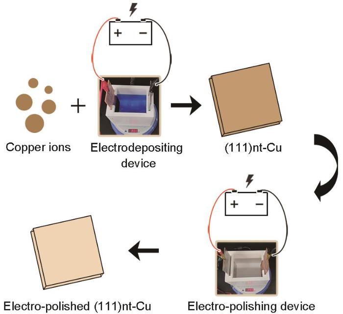
图1
(111)取向纳米孪晶Cu ((111)nt-Cu)样品制备的电镀工艺流程
Fig.1
Electroplating process for the deposition of (111)-oriented nanotwinned copper ((111)nt-Cu)
1.2 电解抛光
电解抛光的目的是对Cu基体表面的粗糙度进行控制,使得(111)nt-Cu和C-Cu 2种样品的粗糙度处在相近的水平。电解抛光前,使用KEYENCE 3D激光共聚焦显微镜测量(111)nt-Cu样品的表面粗糙度(Ra)约为273 nm,C-Cu样品的Ra约为81 nm,因此需要通过电解抛光工艺使得(111)nt-Cu样品的Ra降至C-Cu样品的同级水平。
根据YB/T 4377-2014 《金属试样的电解抛光方法》,配置500 mL的电解液倒入定制的聚四氟乙烯电解槽中,其中85%H3PO4与纯H2O的体积比为7∶3。钛板上固定(111)nt-Cu样品作为阳极,使用含(0.035~0.065)%P (质量分数)的铜板作为阴极。电源设置为1.2~1.8 V的恒电压模式,磁力搅拌器的转速设置为200~350 r/min,抛光时间为12 min。电解抛光后,(111)nt-Cu样品的Ra约为83.17 nm,达到与C-Cu样品相近水平。
1.3 高温氧化实验
空气气氛下,将2种样品放置于加热台上,加热台温度设置为250℃。每隔3 min取样观察,得到不同氧化时间(0、3、6、9和12 min)下(111)nt-Cu和C-Cu样品。使用SEM以5 keV的加速电压及二次电子(SE)成像模式观察氧化后Cu基体的表面状态、氧化层厚度及其截面微观形貌。其中氧化层的厚度由ImageJ软件测量得出。使用ESCALAB 250Xi X 射线光电子能谱(XPS)分析氧化物成分和厚度,以Ta2O5为标定物对溅射速率进行标定,溅射速率为0.5 nm/s,每隔40 s 测量样品中Cu和O的含量,溅射时间共400 s,溅射深度为200 nm。同时,分别使用SCIOS FIB和F200X透射电子显微镜(TEM)对氧化后(111)nt-Cu和C-Cu的截面组织和表面形貌进行表征。
针对同一批样品,对Cu基体氧化前后的表面颜色进行了对比记录。在一个可控光照环境的摄影棚中,使用相同的拍照设定,对样品进行同角度的俯视拍摄,旨在最真实地反映Cu基体氧化前后的颜色变化。
根据本课题前期结果[33],由于(111)nt-Cu本身的特性,本工作中设计的250℃的短时间氧化实验对其微观组织(包括织构、晶粒尺寸和过渡层厚度)均无明显影响。
1.4 润湿性实验
为保证每次印刷的焊膏(SAC305)体积相等,使用定制钢网作为辅助工具,分别给(111)nt-Cu和C-Cu样品印刷商用焊锡膏。将印刷完焊锡膏的样品放置于充满N2保护的封闭加热台上,加热台温度设置为250℃,加热1.5 min使焊料完全融化并且铺展成型。
使用VK-X3000 3D激光共聚焦显微镜对焊点进行扫描,生成焊点的轮廓图、高度曲线和3D图像,从而拟合出焊点的铺展面积,同时测得焊点在Cu基体表面的接触角。
2 实验结果
2.1 Cu基体加热氧化的表面颜色变化
加热过程中(111)nt-Cu和C-Cu样品表面的颜色变化如图2所示。经过12 min的氧化,(111)nt-Cu样品Cu基体表面的颜色由光亮的铜黄色变为暗橘色,表面有部分暗赤色斑点,C-Cu样品Cu基体表面的颜色由光亮的铜黄色完全变为暗赤色。研究[34,35]表明,Cu的氧化层厚度与表面颜色有着对应关系。本工作中,经过12 min的氧化,(111)nt-Cu样品表面只是生成了部分暗赤色斑点,而C-Cu样品表面形成了连续的暗赤色氧化层,可以初步判定(111)nt-Cu抗氧化性能要优于C-Cu。值得注意的是,由于电镀过程中不可避免地存在电流密度分布的差异,样品表面不同区域的粗糙度存在一定差别,导致氧化过程中Cu基体表面的氧化速率并不完全一致,因此图2所示样品表面颜色分布不够均匀。
图2
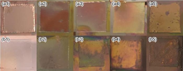
图2
在250℃不同氧化时间下(111)nt-Cu和一般随机取向多晶组织Cu (C-Cu)样品表面的颜色变化(样品尺寸1 cm × 1 cm)
Fig.2
Color changes of the surfaces of (111)nt-Cu (a1-a5) and common randomly oriented equiaxed polycrystalline Cu (C-Cu) (b1-b5) samples after oxidation at 250oC for 0 min (a1, b1), 3 min (a2, b2), 6 min (a3, b3), 9 min (a4, b4), and 12 min (a5, b5) (The dimension of the individule sample is 1 cm × 1 cm)
2.2 Cu氧化层的成分和厚度分析
2种Cu基体氧化后样品表面XPS分析结果如图3所示。根据结合能数据库[36],1价态Cu2p轨道的结合能为932.5 eV,LM2轨道的结合能为570.1 eV;2价态Cu2p轨道的结合能为933.9 eV,LM2轨道的结合能为568.1 eV。由图3可知(以(111)nt-Cu为例),2种Cu基体氧化后表面氧化层的XPS存在结合能为933.9 eV的峰,表明氧化层中存在CuO;也存在结合能为570.1 eV的峰,表明样品氧化层中同时存在Cu2O。图3c 展示了(111)nt-Cu和C-Cu样品O元素含量随氧化层厚度的变化。在200 nm左右的深度,(111)nt-Cu样品氧化层中O元素含量为0,C-Cu样品氧化层中O元素含量为21.9% (原子分数,下同),即C-Cu样品氧化层的厚度要大于(111)nt-Cu样品。且随氧化层深度增加,(111)nt-Cu样品的O元素含量由高于20%平缓下降至0,并没有明显的台阶式骤降,这意味着氧化层中CuO和Cu2O两相没有明显的分层,有共存的可能,这也被后续TEM表征所证实。
图3
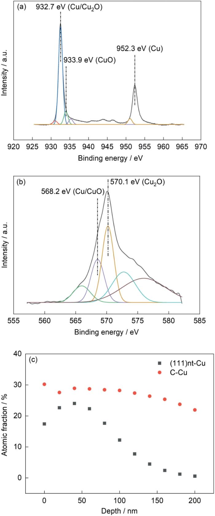
图3
氧化后(111)nt-Cu和C-Cu样品表面的XPS分析
Fig.3
XPS analyses of the surface of (111)nt-Cu and C-Cu samples after oxidation
(a) 2p orbital spectrum of (111)nt-Cu
(b) LM2 orbital spectrum of (111)nt-Cu
(c) depth profiles of the content of O in (111)nt-Cu and C-Cu samples after oxidation
图4为(111)nt-Cu和C-Cu样品氧化层截面的SEM像和FIB像。2个样品均有明显的氧化层/Cu基体的分界线,且(111)nt-Cu样品的氧化层厚度明显小于C-Cu样品。经计算,(111)nt-Cu样品表面氧化层的平均厚度约为121 nm,C-Cu样品表面氧化层的平均厚度约为280 nm。(111)nt-Cu样品氧化层厚度仅为C-Cu样品氧化层厚度的43.2%。
图4
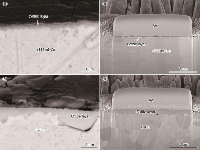
图4
(111)nt-Cu和C-Cu样品氧化层截面的SEM像和FIB像
Fig.4
SEM (a, c) and FIB (b, d) images of the cross sections of (111)nt-Cu (a, b) and C-Cu (c, d) samples after oxidation
图5为2种Cu基体氧化后样品截面的TEM像、HRTEM像和选区电子衍射(SAED)花样。图5a和b分别为(111)nt-Cu和C-Cu样品氧化层截面的TEM明场像。可见,(111)nt-Cu和C-Cu基体氧化后表面均生成组织均匀的氧化层,具有单层衬度并未形成明显的双层结构。图5c和d分别为(111)nt-Cu和C-Cu基体氧化层的HRTEM像。可见2者氧化层均由纳米晶颗粒构成,对应的SAED花样分别如图5e和f所示,可以确定2种Cu基体氧化后的氧化层中同时存在CuO和Cu2O氧化物,而从TEM和HRTEM像中并未观察到明显的CuO/Cu2O分层,说明2种氧化物共存于单层氧化层中,与XPS表征结果一致。这说明在本工作条件下2种基体在氧化过程中同时生成CuO和Cu2O纳米颗粒混合的单层氧化层组织,而非通常的Cu2O/CuO多层结构。
图5
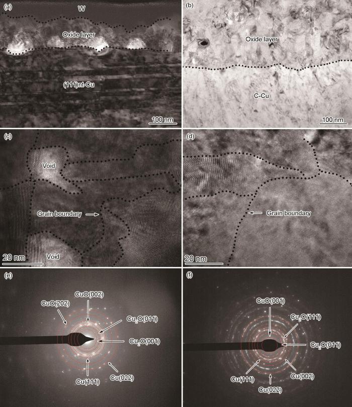
图5
(111)nt-Cu和C-Cu样品氧化层截面的TEM明场像、HRTEM像和选区电子衍射花样
Fig.5
TEM bright field images of the cross sections of (111)nt-Cu (a) and C-Cu (b) samples after oxidation, and the corresponding HRTEM images (c, d) as well as selected area electron diffraction (SAED) patterns (e, f) of the oxide layer
2.3 润湿性
250℃不同氧化时间下焊料与(111)nt-Cu和C-Cu样品氧化层的接触角如图6所示。未氧化时,焊料与(111)nt-Cu和C-Cu样品的接触角相差无几,均在10°左右。氧化开始后,接触角均随着氧化时间的延长而增大,但焊料与(111)nt-Cu之间接触角的增长速率明显更小。在氧化时间为12 min时,焊料与(111)nt-Cu样品表面氧化层之间的接触角为18.7°,焊料与C-Cu样品表面氧化层之间的接触角为25.5°,焊料与(111)nt-Cu样品表面氧化层之间的接触角比焊料与C-Cu样品表面氧化层之间的接触角小26.7%。
图6
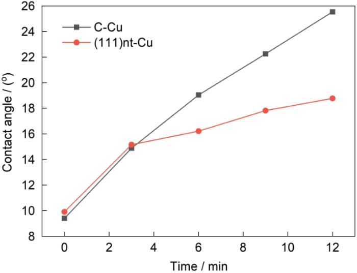
图6
250℃下(111)nt-Cu和C-Cu样品接触角随氧化时间的变化
Fig.6
Contact angles of solder bumps on (111)nt-Cu and C-Cu samples with oxidation time at 250oC
图7
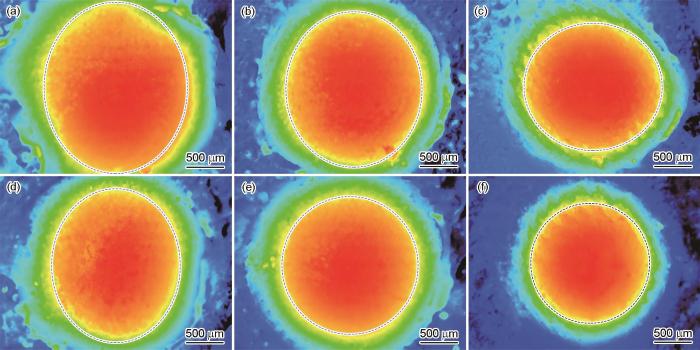
图7
250℃不同氧化时间下焊料在(111)nt-Cu和C-Cu样品表面的铺展面积云图
Fig.7
Spreading cloud images of the solder bump on the surfaces of (111)nt-Cu (a-c) and C-Cu (d-f) samples oxidized at 250oC for 0 min (a, d), 3 min (b, e), and 12 min (c, f)
表1 250℃不同氧化时间下焊料在(111)nt-Cu和C-Cu样品表面的铺展面积 (mm2)
Table 1
| Sample | 0 min | 3 min | 12 min |
|---|---|---|---|
| (111)nt-Cu | 2.639 | 2.276 | 1.896 |
| C-Cu | 2.132 | 2.015 | 1.522 |
3 分析讨论
Cu的氧化过程主要是通过表面化学吸附和反应物离子的扩散进行的[37]。从化学反应角度分析,Cu是fcc结构晶体,只有(111)晶面是密排面,最邻近原子数目多,原子之间的结合力较大,排列紧凑。而原子排列越紧凑,Coulomb能就越低,晶面氧化需要的激活能就越大[38]。相对地,C-Cu的表面具有多种取向,所以其表面上存在大量的高能原子,容易吸附O2发生氧化反应。此外,(111)晶面有比其他晶面更低的表面能(0.45 eV),所以Cu原子从(111)晶面向外扩散是困难的[38]。又因为(111)nt-Cu是高度(111)择优,所以(111)nt-Cu表面Cu原子向外扩散难于进行,导致氧化物生长速率慢。
图8
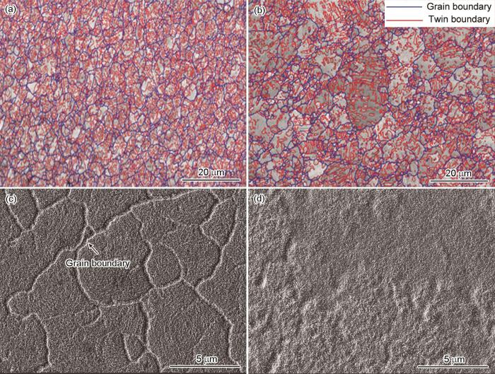
图8
(111)nt-Cu和C-Cu样品表面氧化前的EBSD像和氧化后的FIB像
Fig.8
EBSD images of the original surfaces of (111)nt-Cu (a) and C-Cu (b) samples showing the grain boundry and twin boundary in the normal direction, as well as those of FIB surface images (c, d) after oxidation
表2 (111)nt-Cu和C-Cu样品的晶界统计信息
Table 2
| Sample | Area fraction of LAGB % | Area fraction of HAGB % | Grain boundary length μm | Twin boundary length μm |
|---|---|---|---|---|
| (111)nt-Cu | 11.1 | 88.9 | 5621 | 13814 |
| C-Cu | 0.9 | 99.1 | 2536 | 7109 |
图8c和d分别为(111)nt-Cu和C-Cu样品表面氧化后的FIB像。可见,(111)nt-Cu和C-Cu氧化后表面均形成颗粒状的氧化覆盖物,其中(111)nt-Cu样品表面中柱状晶晶界更加清晰一些(图8c)。如前所述,(111)晶面更低的表面能使得Cu原子从(111)nt-Cu晶体内部向外扩散,晶界是最快的扩散通道,且(111)nt-Cu有着较大的晶界长度和孪晶界长度,因此(111)nt-Cu晶界处氧化层厚度明显高于其余位置(图8c中箭头所示)。而C-Cu样品表面存在大量的高能原子,在250℃高温下,Cu原子从晶界扩散相对于晶内扩散的速率差异不再显著,且C-Cu样品有着较小的晶界长度和孪晶界长度,因此C-Cu样品表面的氧化层在晶界处的厚度与其他位置没有明显差异,整体较为平坦均匀(图8d)。由于大角度晶界处的原子排列更加无序,其界面能大于小角度晶界[39],因此Cu原子在大角度晶界的扩散速率要高于小角度晶界。如表2所示,C-Cu样品表面大角度晶界面积分数为99.1%,(111)nt-Cu样品的大角度晶界面积分数为88.9%,小于C-Cu样品。所以,C-Cu样品中比例更高的大角度晶界为Cu原子从Cu基体内部向表面扩散提供了大量的“快速通道”,因此C-Cu样品的氧化层厚度要大于(111)nt-Cu样品。
从晶界的取向差角度来看,(111)nt-Cu样品氧化前Cu基体表面的晶界取向差分布全部为取向差角小于5°的小角度晶界和取向差角为60°的孪晶界,如图9a所示。而在C-Cu样品氧化前的Cu基体表面,取向差角30°~40°的晶界具有一定比例,如图9b所示。这是因为,(111)nt-Cu样品在自然生长方向上具有高的(111)择优性,而C-Cu样品则没有择优取向,所以C-Cu样品中的晶界取向差角较为杂乱。这里有2点值得关注:(1) C-Cu和(111)nt-Cu样品都含有高比例的孪晶界(取向差角为60°),但是孪晶界的界面在原子尺度上是平滑的,其界面能远小于其他取向差角的晶界,例如,孪晶界与普通晶界的界面能分别为0.045和0.645 J/m2 [39];(2) 在(111)nt-Cu样品中,由于存在竖直的柱状晶组织(图10a),充满了晶界和孪晶界的“交汇点”,而这种“交汇点”会极大地限制Cu原子从Cu基体内部向表面扩散[40]。因此,(111)nt-Cu和C-Cu样品氧化前Cu基体表面大量取向差角为60°的孪晶界并不会促进Cu原子向表面迁移,从而促进氧化。相反地,C-Cu样品中一定比例的取向差角30°~40°的晶界,可能在氧化过程中起到了促进Cu原子向表面扩散的重要作用。综上可知,相同条件下(111)nt-Cu样品的氧化层薄于C-Cu样品。
图9
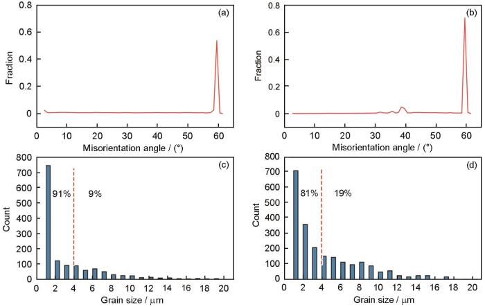
图9
(111)nt-Cu和C-Cu样品氧化前表面的晶粒取向差角分布和晶粒尺寸分布
Fig.9
Grain misorientation distributions (a, b) and grain size distributions (c, d) of (111)nt-Cu (a, c) and C-Cu (b, d) samples
图10
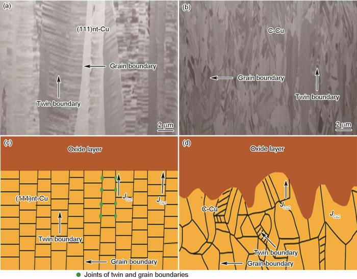
图10
氧化前(111)nt-Cu和C-Cu样品截面的FIB像以及Cu在晶界处扩散的示意图
Fig.10
Cross section FIB images of electroplated (111)nt-Cu (a) and C-Cu (b) samples; diffution illustrations of Cu atom on grain boundaries in (111)nt-Cu (c) and C-Cu (d) samples (JCu1—Cu diffusion flux in (111)nt-Cu along the grain boundary; JCu2—Cu diffusion flux in C-Cu along the grain bounadry)
图10给出了氧化机理示意图。图10a和b分别为(111)nt-Cu和C-Cu样品氧化前的截面FIB像。(111)nt-Cu样品由柱状晶粒所构成,其每个晶粒中又由致密的孪晶片层构成。C-Cu样品由尺寸和取向不均一的等轴晶粒所构成,部分晶粒中也有孪晶片层。(111)nt-Cu样品氧化前Cu基体中存在大量的孪晶界和柱状晶界的“交汇点”,与C-Cu样品相比,这种“交汇点”可以有效抑制Cu从晶界向表面扩散(图10c中的JCu1为(111)nt-Cu中的Cu原子由Cu基体内部向Cu基体/氧化层界面扩散的通量)。而C-Cu样品的晶粒取向和尺寸不均匀。所以,C-Cu样品中的Cu的扩散会因为晶界的取向差角不同以及晶粒取向的不同而变化很大(图10d中的JCu2为C-Cu中的Cu原子由Cu基体内部向Cu基体/氧化层界面扩散的通量)。
综合以上氧化机理的解释可知,(111)nt-Cu与C-Cu样品抗氧化性能的差异是由Cu原子向外扩散的速率差异引起的。一方面,(111)晶面较低的表面能使得(111)nt-Cu样品的氧化需要更大的激活能,降低了(111)nt-Cu样品中Cu原子向外的扩散速率,且(111)nt-Cu样品内部具有更低界面能的孪晶界与晶界产生了大量的“交汇点”,进一步降低了(111)nt-Cu样品中Cu原子向外的扩散速率;另一方面,原子在晶体内扩散,晶界为扩散速率最快的通道,且原子在大角度晶界的扩散速率高于小角度晶界。与C-Cu样品相比,(111)nt-Cu样品大角度晶界面积分数更小,限制了(111)nt-Cu样品的氧化。
虽然Cu的氧化与Cu的向外扩散和O的向内扩散均有关[41],但由于Cu基体本身的差异所导致的氧化层不同已经足够明显,因此本工作没有关注O的内扩散。
4 结论
(1) (111)nt-Cu和C-Cu 2种Cu基体在氧化过程中表面均出现了由光亮到暗淡的颜色变化。其中,(111)nt-Cu样品的颜色变化速率慢于C-Cu样品,说明(111)nt-Cu样品的抗氧化能力优于C-Cu样品。在250℃条件下加热9 min后,2种Cu基体中同时存在CuO和Cu2O 2种氧化物,且以纳米颗粒的形式共存而未分层。
(2) 在250℃条件下加热9 min后,(111)nt-Cu样品氧化层平均厚度约为121 nm,C-Cu样品氧化层厚度约为280 nm。这是Cu原子沿晶界向外扩散的速率差异导致的。引起这种速率差异的原因有2个:一是因为(111)晶面有着更低的表面能,Cu原子扩散较难;二是因为C-Cu样品表面的大角度晶界所占比例要高于(111)nt-Cu样品,且C-Cu样品表面存在大量取向差角30°~40°的晶界。这些具有高界面能的界面导致C-Cu样品氧化层厚度大于(111)nt-Cu样品。
(3) 得益于(111)nt-Cu样品良好的抗氧化性能,(111)nt-Cu样品的焊料润湿性优于C-Cu样品,其润湿角相差26.7%。
参考文献
Effect of methylene blue on the microstructure and mechanical properties of nanotwinned copper during DC electroplating
[J].
亚甲基蓝对直流电镀纳米孪晶铜组织及力学性能的影响
[J].
Wafer-level bonding/stacking technology for 3D integration
[J].
The oxidation of copper at 200-900oC
[J].
铜在200~900℃的氧化
[J].
Low-temperature oxidation of Cu(100), Cu(110) and Cu(111)
[J].
The rates of oxidation of several faces of a single crystal of copper as determined with elliptically polarized light
[J].
Unidirectional growth of microbumps on (111)-oriented and nanotwinned copper
[J].
Ultrahigh strength and high electrical conductivity in copper
[J].Methods used to strengthen metals generally also cause a pronounced decrease in electrical conductivity, so that a tradeoff must be made between conductivity and mechanical strength. We synthesized pure copper samples with a high density of nanoscale growth twins. They showed a tensile strength about 10 times higher than that of conventional coarse-grained copper, while retaining an electrical conductivity comparable to that of pure copper. The ultrahigh strength originates from the effective blockage of dislocation motion by numerous coherent twin boundaries that possess an extremely low electrical resistivity, which is not the case for other types of grain boundaries.
Tensile properties of Cu with deformation twins induced by SMAT
[J].

High density nano-scale deformation twins were introduced in the surface layer of Cu sample by means of surface mechanical attrition treatment (SMAT) at room temperature. The Cu sample with deformation twins shows a yield strength of about 470 MPa in tension tests. The significant strengthening may be attributed to the effective inhibition of slip dislocations by abundant twin boundaries.
Strengthening materials by engineering coherent internal boundaries at the nanoscale
[J].Strengthening materials traditionally involves the controlled creation of internal defects and boundaries so as to obstruct dislocation motion. Such strategies invariably compromise ductility, the ability of the material to deform, stretch, or change shape permanently without breaking. Here, we outline an approach to optimize strength and ductility by identifying three essential structural characteristics for boundaries: coherency with surrounding matrix, thermal and mechanical stability, and smallest feature size finer than 100 nanometers. We assess current understanding of strengthening and propose a methodology for engineering coherent, nanoscale internal boundaries, specifically those involving nanoscale twin boundaries. Additionally, we discuss perspectives on strengthening and preserving ductility, along with potential applications for improving failure tolerance, electrical conductivity, and resistance to electromigration.
Revealing the maximum strength in nanotwinned copper
[J].The strength of polycrystalline materials increases with decreasing grain size. Below a critical size, smaller grains might lead to softening, as suggested by atomistic simulations. The strongest size should arise at a transition in deformation mechanism from lattice dislocation activities to grain boundary-related processes. We investigated the maximum strength of nanotwinned copper samples with different twin thicknesses. We found that the strength increases with decreasing twin thickness, reaching a maximum at 15 nanometers, followed by a softening at smaller values that is accompanied by enhanced strain hardening and tensile ductility. The strongest twin thickness originates from a transition in the yielding mechanism from the slip transfer across twin boundaries to the activity of preexisting easy dislocation sources.
Bottom-up electrodeposition of large-scale nanotwinned copper within 3D through silicon via
[J].
Low-resistance and high-strength copper direct bonding in no-vacuum ambient using highly (111)-oriented nano-twinned copper
[A].
Low-temperature direct copper-to-copper bonding enabled by creep on (111) surfaces of nanotwinned Cu
[J].
Predicting trends in rate parameters for self-diffusion on FCC metal surfaces
[J].
Microstructure control of unidirectional growth of η-Cu6Sn5 in microbumps on 〈111〉 oriented and nanotwinned Cu
[J].
The self-healing of Kirkendall voids on the interface between Sn and (111) oriented nanotwinned Cu under thermal aging
[J].
Comparison of oxidation in uni-directionally and randomly oriented Cu films for low temperature Cu-to-Cu direct bonding
[J].
Micro-cones Cu fabricated by pulse electrodeposition for solderless Cu-Cu direct bonding
[J].
Study on microstructure and hardness of direct-current electrodeposited nanotwinned Cu
[J].
直流电解沉积纳米孪晶铜的微观结构与硬度研究
[J].
The effect of transition layer on the strength of nanotwinned copper film by DC electrodeposition
[A].
Regulating the orientation and distribution of nanotwins by trace of gelatin during direct current electroplating copper on titanium substrate
[J].
Investigation on mechanical properties of nanotwinned diamond and nanotwinned copper
[D].
纳米孪晶金刚石和纳米孪晶铜的力学性质研究
[D].
Stabilizing nanostructures in metals using grain and twin boundary architectures
[J].
Nanotwinned and hierarchical nanotwinned metals: A review of experimental, computational and theoretical efforts
[J].
Fatigue fracture analysis of nano-twinned copper under cyclic tensile loading
[D].
循环拉伸载荷下纳米孪晶铜的疲劳断裂分析
[D].
Dislocation characterization in fatigued Cu with nanoscale twins
[J].
Atomistic mechanisms of fatigue in nanotwinned metals
[J].
History-independent cyclic response of nanotwinned metals
[J].
Extra strengthening and work hardening in gradient nanotwinned metals
[J].
The mechanical property and microstructural thermal stability of gradient-microstructured nanotwinned copper films electroplated on the high (111)-orientated sub-strates
[J].
Electrodeposition and growth mechanism of preferentially orientated nanotwinned Cu on silicon wafer substrate
[J].
Electroplating nanotwinned copper for ultrafine pitch redistribution layer (RDL) of advanced packaging technology
[A].
Research on preparation and reliability of nanotwinned copper interconnect materials for microelectronic packaging
[D].
微电子封装用纳米孪晶铜互连材料的制备及可靠性研究
[D].
Copper and its alloy
[J].
銅·銅合金
[J].
Regarding discoloration of copper and copper alloys
[J].
銅および銅合金の変色について
[J].
Resolving surface chemical states in XPS analysis of first row transition metals, oxides and hydroxides: Sc, Ti, V, Cu and Zn
[J].
Study on the oxidation behavior of single crystal copper
[D].
单晶铜氧化行为的研究
[D].
Growth mechanisms of Cu3Sn on polycrystalline and single crystalline Cu substrates
[J].
Growth mechanism of interfacial IMCs on (111) preferred orientation nanotwinned Cu UBM for 3D IC packaging
[A].
Comparison of the oxidation behavior of nanocrystalline and coarse-grain copper
[J].
Inhibition of intermetallic compounds growth at Sn-58Bi / Cu interface bearing CuZnAl memory particles (2-6 μm)
[J].
