Center for Alloy Innovation and Design (CAID), State Key Laboratory for Mechanical Behavior of Materials, Xi'an Jiaotong University, Xi'an 710049, China
In the era of big data, the demand for data storage and processing is increasing because of advanced technologies such as artificial intelligence (AI), 5G, and cloud computing. Emerging non-volatile memory materials and devices present remarkable opportunities to enhance computing capacity. Concurrently, the AI-driven scientific research paradigm introduces a new mode for improving device performance. This review focuses on recent advances in phase-change memory materials and devices, emphasizing computational- and data-driven methodologies. Phase-change materials (PCMs) operate based on rapid and reversible phase transitions between amorphous and crystalline states, where differences in electrical and optical properties are used to encode digital information. These materials typically consist of multicomponent alloys, with phase transitions involving melting, quenching, crystallization, glass relaxation, and crystal-crystal structural changes. To achieve a detailed atomistic understanding of PCMs, large-scale density functional theory (DFT) and DFT-based ab initio molecular dynamics (AIMD) simulations are essential. Comparisons between DFT/AIMD simulations and experimental results have clarified many fundamental aspects of PCM. The first part of this review provides an overview of the history and progress in large-scale ab initio simulations of PCMs. With atomic-scale knowledge, rational materials design becomes feasible. The second part explores methods for developing new PCMs with specific properties, such as accelerating crystallization at elevated temperatures while maintaining non-volatile characteristics at room temperature. High-throughput screening's role in discovering new phase change alloys is also discussed. In the third part, we examine multiscale and cross-scale simulations of PCM for various optical and electronic phase change applications. By computing the dielectric functions of PCM during the amorphous-to-crystalline transition, we can track changes in the refractive index and extinction coefficient across visible and infrared spectra over time. These DFT-computed parameters inform coarse-grained device simulations using finite-difference time-domain (FDTD) or finite element method (FEM). Based on these multiscale simulations, we offer optimization guidelines for non-volatile color display and photonic waveguide devices. The machine learning potentials address some performance gaps between the DFT/AIMD and FEM/FDTD calculations. Machine-learning-driven molecular dynamics (MLMD) simulations serve as cross-scale simulations, with recent developments including neural networks, graph convolutional neural networks, and Gaussian approximation potentials. We discuss the role of MLMD in enabling device-scale atomistic simulations, facilitating device design and optimization with atomic-scale information. Finally, we outline future opportunities and challenges in theoretical PCM research. With ongoing AI-driven fundamental research, we anticipate the commercialization of high-performance phase change memory, neuroinspired computing, and reconfigurable nanophotonic devices, which will, in turn, foster the development of more advanced theoretical tools for research.
Fig.2
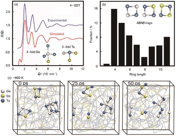
Ab initio molecular dynamic (AIMD) modeling of amorphous Ge2Sb2Te5 phase-change material (a, b) structure factor (a) and ring lengths (b) distribution calculated at 300 K[53] ( Q —scattering vector, S( Q )—X-ray scattering factor, a-GST—amorphous GST, ABAB—ABAB rings, A: Ge/Sb, B: Te) (c) evolution of ABAB rings calculated at about 600 K[56]
Fig.3
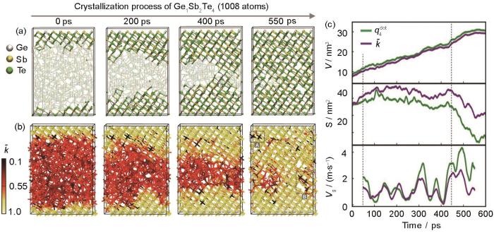
AIMD crystallization simulations of a 1008-atom Ge1Sb2Te4 model at about 600 K[61]
(a) snapshots of the crystallization process identified by
(b) snapshots of the crystallization process identified by smooth overlap of atomic positions (SOAP) kernel (—SOAP kernel function)
(c) structural analyses of the crystallization process (V—volume of the crystalline region, S—area of the interface between amorphous and crystalline regions, Vg—crystal growth velocity, —local order parameter)
Fig.4
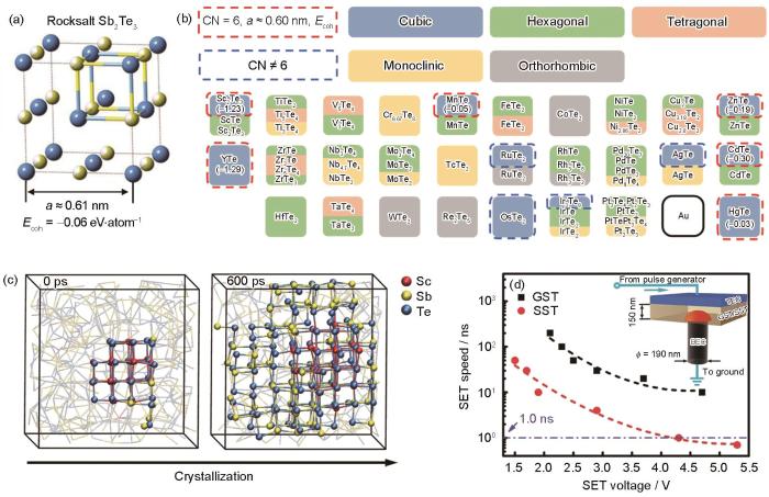
Design of Sc0.2Sb2Te3 phase-change alloy with ultrafast nucleation rate and device validation[56]
(a) structure of rocksalt Sb2Te3 (Ecoh—cohesive energy, a—cell length, the yellow spheres represent the sublattice occupied by Sb atoms and vacancies with a ratio of 2∶1, the blue spheres represent the sublattice occupied by Te atoms)
(b) materials screening (CN—coordination number)
(c) crystallization process
(d) SET speed (GST—Ge2Sb2Te5, SST—Sc0.2Sb2Te3. Inset shows the schematic of the T type phase change device, TEC—top electrode contact, BEC—bottom electrode contact, ϕ—diameter of BEC)
Fig.6
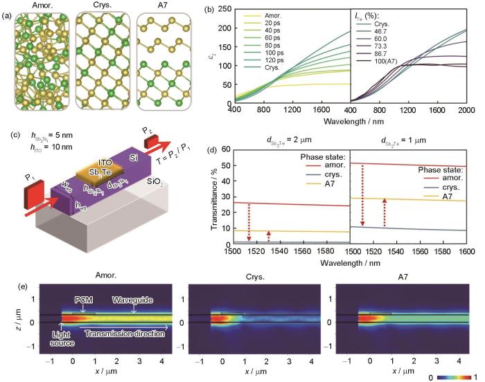
Multiscale simulation of Sb2Te1 phase change alloy for waveguide devices [111]
(a) local structural snapshots of amorphous and crystalline Sb2Te1 (amor.—amorphous; crys.—crystalline; Sb and Te atoms are rendered as yellow and green spheres, respectively)
(b) changes in dielectric function upon crystallization and Te ordering (ε2—imaginary part of the dielectric function, ITe—concentration of Te atoms in Te-rich layers)
(c) schematic of a Sb2Te1 waveguide device (ITO—indium tin oxide, —height of ITO, —height of Sb2Te1 layer, —length of Sb2Te1 layer, wwg—width of the waveguide, hwg—height of the waveguide, T—transmittance, P1—power of incident light, P2—power of transmitted light)
(d) transmittance profiles of different phases
(e) corresponding electric field |E| of the x-z plane of Sb2Te1 device in different phases, the color bar below shows the normalized electric field intensity (PCM—phase-change materials)
Wang等[111]将DFT计算得到的Sb2Te1的光学性质作为关键参数传递至FDTD仿真软件Lumerical[113]并进行了光学器件模拟。硅光技术的快速发展为PCM光子器件的大规模集成带来了新的契机。图6c[111]给出了典型的PCM光波导器件,该器件由SiO2绝缘体、绝缘体上硅波导(silicon-on-insulator,SOI)、沉积在硅波导上的相变薄膜与氧化铟锡(indium tin oxide,ITO)覆盖层构成。入射光信号沿着硅波导传播时会与相变薄膜之间发生倏逝耦合形成倏逝场,由于相变薄膜在不同相态下具有不同的消光系数,入射光未能被全反射的部分被不同程度地吸收。当入射光强度较大时,相变材料吸收能量产生的Joule热足以诱发材料相变,完成对信息的编码;当入射光强度适中时,材料的相态不会发生改变,通过测量经过相变薄膜区域后出射光的光强度便可完成对信息的读取。图6d[111]给出了长度为2与1 μm的Sb2Te1波导器件光透过率的FDTD仿真结果,在长度为1 μm器件中透过率对比窗口最大可达40%,超越了Ge-Sb-Te光波导器件约20%[28]。图6e[111]分别对应了Sb2Te1合金3种结构的电场|E|分布图,直观地展示了处于不同相态的波导器件的光透过程度。需注意的是,当Sb2Te1的透射率差异最大时,晶体相为无序菱方结构,而Te有序化会减小该窗口,即额外的升温退火处理会减弱Sb2Te1波导器件的性能。因此,在使用该类器件时应当进行高频高速的器件操作,并且降低环境温度的干扰。该工作是多尺度模拟指导PCM光学应用研究的典型案例。近期,Zheng等[114]通过原位电子显微学实验,报道了Sb2Te1存在无序菱方亚稳相以及其向稳定有序A7层状结构转变的微观演化过程,证实了Wang等[111]AIMD的计算结果。
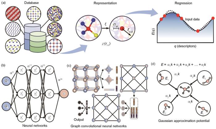
机器学习势的具体拟合过程如图7a[97]所示,主要包括3大步骤:参考数据库的建立、原子环境量化和势能面拟合。依据拟合目标建立全面而精准的数据库是机器学习势的基础。数据库中的参考结构需要具有代表性,不仅能够特征化描述势能面上能量极小值点的结构,还要包含高能量的结构信息,以通过有限数量的原子构型实现对势能面的充分采样。常见的参考数据库来源包括Materials Project[48]、ICSD[115]等材料数据库,AIMD模拟计算,势能迭代训练过程中的结构,以及从头算随机晶体结构搜索(ab initio random structure searching,AIRSS)[116]等。数据库中的结构需要通过DFT进行精确的计算来获取体系中原子的能量和受力信息。完成数据采集后,如何将数据库中体系的空间构型转化为机器学习可识别的数据集,即采用数学表达方式量化原子环境,是下一个核心的问题。该量化指标被称为材料描述符,可以提炼原子局部环境的关键信息,便于高效重构原子环境。一般情况下,某一原子环境的描述符以该原子为中心,将指定截断半径内近邻原子的信息编码,且需要在满足平移、旋转、置换等空间不变性的前提下兼顾计算效率与连贯性。势能面的拟合则是对构型原子环境与能量受力数据的回归过程,通过不断地回归学习减小目标势能面与DFT数据点之间的差异。MLMD通常使用LAMMPS软件进行计算[117]。
Fig.7
Process and method for fitting machine learning interatomic potential
(a) construction process of machine learning interatomic potential, according to Ref.[97] (—process of getting the smooth overlap of atomic positions descriptor, σat—smooth parameter, rcut—specified cutoff, ρi (rcut)—obtained atomic density, q—descriptors, E(q)—energies; the red, blue and yellow spheres represent Ge, Te and Sb atoms, respectively)
(b) sketch of the neural, networks according to Ref.[118] ( G1, G2—input vectors describing the atomic configurations, —weight sum of the node values, αij —connecting weight parameter, ɛ—potential energy)
(c) schematic of the graph convolutional neural networks[119]
(d) schematic of the kernel based Gaussian approximation potential, according to Ref.[37] (Ei —potential energy, αi —regression coefficient, k—SOAP similarity)
Phase-change materials are some of the most promising materials for data-storage applications. They are already used in rewriteable optical data storage and offer great potential as an emerging non-volatile electronic memory. This review looks at the unique property combination that characterizes phase-change materials. The crystalline state often shows an octahedral-like atomic arrangement, frequently accompanied by pronounced lattice distortions and huge vacancy concentrations. This can be attributed to the chemical bonding in phase-change alloys, which is promoted by p-orbitals. From this insight, phase-change alloys with desired properties can be designed. This is demonstrated for the optical properties of phase-change alloys, in particular the contrast between the amorphous and crystalline states. The origin of the fast crystallization kinetics is also discussed.
WongH S P, RaouxS, KimS, et al.
Phase change memory
[J]. Proc. IEEE, 2010, 98: 2201
ZhangW, MazzarelloR, WuttigM, et al.
Designing crystallization in phase-change materials for universal memory and neuro-inspired computing
The global demand for data storage and processing has increased exponentially in recent decades. To respond to this demand, research efforts have been devoted to the development of non-volatile memory and neuro-inspired computing technologies. Chalcogenide phase-change materials (PCMs) are leading candidates for such applications, and they have become technologically mature with recently released competitive products. In this Review, we focus on the mechanisms of the crystallization dynamics of PCMs by discussing structural and kinetic experiments, as well as ab initio atomistic modelling and materials design. Based on the knowledge at the atomistic level, we depict routes to improve the parameters of phase-change devices for universal memory. Moreover, we discuss the role of crystallization in enabling neuro-inspired computing using PCMs. Finally, we present an outlook for future opportunities of PCMs, including all-photonic memories and processors, flexible displays with nanopixel resolution and nanoscale switches and controllers.
ZhouW, ShenX Y, YangX L, et al.
Fabrication and integration of photonic devices for phase-change memory and neuromorphic computing
[J]. Int. J. Extrem. Manuf., 2024, 6: 022001
ZhangZ H, WangZ W, ShiT, et al.
Memory materials and devices: From concept to application
Memristors are continuously tunable resistors that emulate biological synapses. Conceptualized in the 1970s, they traditionally operate by voltage-induced displacements of matter, although the details of the mechanism remain under debate. Purely electronic memristors based on well-established physical phenomena with albeit modest resistance changes have also emerged. Here we demonstrate that voltage-controlled domain configurations in ferroelectric tunnel barriers yield memristive behaviour with resistance variations exceeding two orders of magnitude and a 10 ns operation speed. Using models of ferroelectric-domain nucleation and growth, we explain the quasi-continuous resistance variations and derive a simple analytical expression for the memristive effect. Our results suggest new opportunities for ferroelectrics as the hardware basis of future neuromorphic computational architectures.
Memristive devices are electrical resistance switches that can retain a state of internal resistance based on the history of applied voltage and current. These devices can store and process information, and offer several key performance characteristics that exceed conventional integrated circuit technology. An important class of memristive devices are two-terminal resistance switches based on ionic motion, which are built from a simple conductor/insulator/conductor thin-film stack. These devices were originally conceived in the late 1960s and recent progress has led to fast, low-energy, high-endurance devices that can be scaled down to less than 10 nm and stacked in three dimensions. However, the underlying device mechanisms remain unclear, which is a significant barrier to their widespread application. Here, we review recent progress in the development and understanding of memristive devices. We also examine the performance requirements for computing with memristive devices and detail how the outstanding challenges could be met.
Traditional von Neumann computing systems involve separate processing and memory units. However, data movement is costly in terms of time and energy and this problem is aggravated by the recent explosive growth in highly data-centric applications related to artificial intelligence. This calls for a radical departure from the traditional systems and one such non-von Neumann computational approach is in-memory computing. Hereby certain computational tasks are performed in place in the memory itself by exploiting the physical attributes of the memory devices. Both charge-based and resistance-based memory devices are being explored for in-memory computing. In this Review, we provide a broad overview of the key computational primitives enabled by these memory devices as well as their applications spanning scientific computing, signal processing, optimization, machine learning, deep learning and stochastic computing.
XuM, MaiX L, LinJ, et al.
Recent advances on neuromorphic devices based on chalcogenide phase-change materials
[J]. Adv. Funct. Mater., 2020, 30: 2003419
ShastriB J, TaitA N, Ferreira de LimaT, et al.
Photonics for artificial intelligence and neuromorphic computing
Neuromorphic photonics has recently emerged as a promising hardware accelerator, with significant potential speed and energy advantages over digital electronics for machine learning algorithms, such as neural networks of various types. Integrated photonic networks are particularly powerful in performing analog computing of matrix-vector multiplication (MVM) as they afford unparalleled speed and bandwidth density for data transmission. Incorporating nonvolatile phase-change materials in integrated photonic devices enables indispensable programming and in-memory computing capabilities for on-chip optical computing. Here, we demonstrate a multimode photonic computing core consisting of an array of programable mode converters based on on-waveguide metasurfaces made of phase-change materials. The programmable converters utilize the refractive index change of the phase-change material GeSbTe during phase transition to control the waveguide spatial modes with a very high precision of up to 64 levels in modal contrast. This contrast is used to represent the matrix elements, with 6-bit resolution and both positive and negative values, to perform MVM computation in neural network algorithms. We demonstrate a prototypical optical convolutional neural network that can perform image processing and recognition tasks with high accuracy. With a broad operation bandwidth and a compact device footprint, the demonstrated multimode photonic core is promising toward large-scale photonic neural networks with ultrahigh computation throughputs.
The rapidly growing demand for data storage and processing, driven by artificial intelligence (AI) and other data-intensive applications, is posing a serious challenge for current computing devices based on the von Neumann architecture. For every calculation, data sets need to be shuffled sequentially between the processor, and multiple memory and storage units through bandwidth-limited and energy-inefficient interconnects, typically causing 40% power wastage. Phase-change materials (PCMs) show great promise to break this bottleneck by enabling nonvolatile memory devices that can optimize the complex memory hierarchy, and neuro-inspired computing devices that can unify computing with storage in memory cells. The articles in this issue of MRS Bulletin highlight recent breakthroughs in the fundamental materials science, as well as electronic and photonic implementations of these novel devices based on PCMs.
CurtaroloS, HartG L W, NardelliM B, et al.
The high-throughput highway to computational materials design
High-throughput computational materials design is an emerging area of materials science. By combining advanced thermodynamic and electronic-structure methods with intelligent data mining and database construction, and exploiting the power of current supercomputer architectures, scientists generate, manage and analyse enormous data repositories for the discovery of novel materials. In this Review we provide a current snapshot of this rapidly evolving field, and highlight the challenges and opportunities that lie ahead.
XieJ X, SuY J, XueD Z, et al.
Machine learning for materials research and development
The rapid advancement of big data and artificial intelligence has resulted in new data-driven materials research and development (R&D), which has achieved substantial progress. This fourth paradigm is believed to improve materials design efficiency and industrialized application and stimulate the discovery of new materials. The focus of this work is on the emerging field of machine learning-assisted material R&D, with an emphasis on machine learning predictions and optimization design. Following a brief description of feature construction and selection, recent developments in material predictions on phases/structures, processing-structure-property relationships, microstructure, and material performance are reviewed. This paper also summarizes the research progress on optimization algorithms with machine learning models, which is expected to overcome the bottlenecks such as the small size and high noise level of material data samples and huge space for exploration. The challenges and future opportunities for machine learning applications in materials R&D are discussed and prospected.
The choice of simulation methods in computational materials science is driven by a fundamental trade-off: bridging large time- and length-scales with highly accurate simulations at an affordable computational cost. Venturing the investigation of complex phenomena on large scales requires fast yet accurate computational methods. We review the emerging field of machine-learned potentials, which promises to reach the accuracy of quantum mechanical computations at a substantially reduced computational cost. This Review will summarize the basic principles of the underlying machine learning methods, the data acquisition process and active learning procedures. We highlight multiple recent applications of machine-learned potentials in various fields, ranging from organic chemistry and biomolecules to inorganic crystal structure predictions and surface science. We furthermore discuss the developments required to promote a broader use of ML potentials, and the possibility of using them to help solve open questions in materials science and facilitate fully computational materials design.
LiH, XuY, DuanW H.
Ab initio artificial intelligence: Future research of Materials Genome Initiative
Materials genome engineering (MGE) is a frontier technology in the field of material science and engineering, which is well capable to revolutionize the research and development (R&D) mode of new materials, greatly improve the R&D efficiency, shorten the R&D time, and reduce the cost. This paper reviews the progress of MGE in China from the aspects of the fundamental theory and methods, key technology and equipment, the R&D of new materials and related engineering application, talents training, formation and promotion of new concept of material genetic engineering. The paper also looks forward to the future development of MGE in China.
High-entropy alloys are solid solutions of multiple principal elements that are capable of reaching composition and property regimes inaccessible for dilute materials. Discovering those with valuable properties, however, too often relies on serendipity, because thermodynamic alloy design rules alone often fail in high-dimensional composition spaces. We propose an active learning strategy to accelerate the design of high-entropy Invar alloys in a practically infinite compositional space based on very sparse data. Our approach works as a closed-loop, integrating machine learning with density-functional theory, thermodynamic calculations, and experiments. After processing and characterizing 17 new alloys out of millions of possible compositions, we identified two high-entropy Invar alloys with extremely low thermal expansion coefficients around 2 × 10 per degree kelvin at 300 kelvin. We believe this to be a suitable pathway for the fast and automated discovery of high-entropy alloys with optimal thermal, magnetic, and electrical properties.
XuY F, ElcoroL, SongZ D, et al.
High-throughput calculations of magnetic topological materials
The development of novel materials has experienced three paradigms: purely empirical, theoretical models, and computational materials science. Currently, the huge amount of data generated by experiments and simulations has facilitated a shift in materials science to a data-driven fourth paradigm. Therefore, the development of high-throughput automatic integrated computations and data mining algorithms based on material databases and artificial intelligence algorithms is critical for accelerating the design of novel materials. This paper presents an open-source distributed computational platform called Artificial Learning and Knowledge Enhanced Materials Informatics Engineering 2.0 (ALKEMIE2.0) based on the AMDIV (automation-modular-database-intelligence-visualization) design concepts. The ALKEMIE2.0 platform includes five core components of automation, modular, materials database, artificial intelligence, and visualization, which are suitable for the computational design of novel materials. The overall characteristics of ALKEMIE2.0 are divided into five pillars. ALKEMIE-Core integrates multiscale calculations and simulation software using the ALKEMIE-Plugin application programming interface. Its high-throughput calculation workflows that support 104 magnitude concurrencies are implemented by integrating the automatic frameworks of model constructions, calculation workflows, and data analyses. Furthermore, the platform is based on the ALKEMIE-Server, which can easily and automatically open daemon services and realize information interactions in distributed supercomputers. With its strong portability and scalability, ALKEMIE has been deployed in the National Supercomputing Tianjin Center. In addition, the multitype materials database called the ALKEMIE-Data Vault contains structure, task, workflow, and material property databases, which combined with the power of supercomputing, enables the rapid application of artificial intelligence algorithms in the design of new materials. In particular, the many user-friendly interfaces, which were elaborately designed using the ALKEMIE-GUI and are suitable for scientists with broad backgrounds, make structural building, work flowcharts, data analysis, and machine learning models more transparent and maneuverable. Finally, the main features of ALKEMIE2.0 are demonstrated using two examples of multiplatform deployment and high-throughput screening of binary aluminum alloys.
Differential scanning calorimetry (DSC) is widely used to study the stability of amorphous solids, characterizing the kinetics of crystallization close to the glass-transition temperature T(g). We apply ultrafast DSC to the phase-change material Ge(2)Sb(2)Te(5) (GST) and show that if the range of heating rates is extended to more than 10(4) K s(-1), the analysis can cover a wider temperature range, up to the point where the crystal growth rate approaches its maximum. The growth rates that can be characterized are some four orders of magnitude higher than in conventional DSC, reaching values relevant for the application of GST as a data-storage medium. The kinetic coefficient for crystal growth has a strongly non-Arrhenius temperature dependence, revealing that supercooled liquid GST has a high fragility. Near T(g) there is evidence for decoupling of the crystal-growth kinetics from viscous flow, matching the behaviour for a fragile liquid suggested by studies on oxide and organic systems.
JeyasinghR, FongS W, LeeJ, et al.
Ultrafast characterization of phase-change material crystallization properties in the melt-quenched amorphous phase
Phase change materials are widely considered for application in nonvolatile memories because of their ability to achieve phase transformation in the nanosecond time scale. However, the knowledge of fast crystallization dynamics in these materials is limited because of the lack of fast and accurate temperature control methods. In this work, we have developed an experimental methodology that enables ultrafast characterization of phase-change dynamics on a more technologically relevant melt-quenched amorphous phase using practical device structures. We have extracted the crystallization growth velocity (U) in a functional capped phase change memory (PCM) device over 8 orders of magnitude (10(-10) < U < 10(-1) m/s) spanning a wide temperature range (415 < T < 580 K). We also observed direct evidence of non-Arrhenius crystallization behavior in programmed PCM devices at very high heating rates (>10(8) K/s), which reveals the extreme fragility of Ge2Sb2Te5 in its supercooled liquid phase. Furthermore, these crystallization properties were studied as a function of device programming cycles, and the results show degradation in the cell retention properties due to elemental segregation. The above experiments are enabled by the use of an on-chip fast heater and thermometer called as microthermal stage (MTS) integrated with a vertical phase change memory (PCM) cell. The temperature at the PCM layer can be controlled up to 600 K using MTS and with a thermal time constant of 800 ns, leading to heating rates ∼10(8) K/s that are close to the typical device operating conditions during PCM programming. The MTS allows us to independently control the electrical and thermal aspects of phase transformation (inseparable in a conventional PCM cell) and extract the temperature dependence of key material properties in real PCM devices.
RonnebergerI, ZhangW, EshetH, et al.
Crystallization properties of the Ge2Sb2Te5 phase-change compound from advanced simulations
Phase-change random-access memory (PCRAM) is one of the leading candidates for next-generation data-storage devices, but the trade-off between crystallization (writing) speed and amorphous-phase stability (data retention) presents a key challenge. We control the crystallization kinetics of a phase-change material by applying a constant low voltage via prestructural ordering (incubation) effects. A crystallization speed of 500 picoseconds was achieved, as well as high-speed reversible switching using 500-picosecond pulses. Ab initio molecular dynamics simulations reveal the phase-change kinetics in PCRAM devices and the structural origin of the incubation-assisted increase in crystallization speed. This paves the way for achieving a broadly applicable memory device, capable of nonvolatile operations beyond gigahertz data-transfer rates.
ZhangB, ZhangW, ShenZ J, et al.
Element-resolved atomic structure imaging of rocksalt Ge2Sb2Te5 phase-change material
Cache-type phase-change random-access memory is a remaining challenge on the path to universal memory. The recently designed Sc0.2Sb2Te3 (SST) alloy is one of the most promising phase-change materials (PCMs) to overcome this challenge, as it allows subnanosecond crystallization speed to reach the crystalline ("1") state at elevated temperatures (e.g., 600 K) but years of reliable retention of the amorphous ("0") state for data storage at room temperature. This contrast in kinetics behavior, upon a relatively small temperature excursion, is more dramatic than that in other PCMs. From the temperature dependence of the crystallization kinetics uncovered via ultrafast differential scanning calorimetry, here, we report an apparent fragile-to-strong crossover in the SST supercooled liquid. We illustrate that two factors are at work simultaneously. First, Sc-stabilized precursors serve as heterogeneous sites to catalyze nucleation, reducing the stochasticity and thereby accelerating the nucleation rate. Second, the SST exhibits an enlarged kinetic contrast between elevated and ambient temperatures. Together they constitute a recipe for the design of PCMs that meets the needs of cache-type nonvolatile memory.
HuS W, LiuB, LiZ, et al.
Identifying optimal dopants for Sb2Te3 phase-change material by high-throughput ab initio calculations with experiments
The study of metal-insulator transitions (MITs) in crystalline solids is a subject of paramount importance, both from the fundamental point of view and for its relevance to the transport properties of materials. Recently, a MIT governed by disorder was observed in crystalline phase-change materials. Here we report on calculations employing density functional theory, which identify the microscopic mechanism that localizes the wavefunctions and is driving this transition. We show that, in the insulating phase, the electronic states responsible for charge transport are localized inside regions having large vacancy concentrations. The transition to the metallic state is driven by the dissolution of these vacancy clusters and the formation of ordered vacancy layers. These results provide important insights on controlling the wavefunction localization, which should help to develop conceptually new devices based on multiple resistance states.
JiangT T, WangX D, WangJ J, et al.
In situ characterization of vacancy ordering in Ge-Sb-Te phase-change memory alloys
Multimode silicon photonics is attracting more and more attention because the introduction of higher-order modes makes it possible to increase the channel number for data transmission in mode-division-multiplexed (MDM) systems as well as improve the flexibility of device designs. On the other hand, the design of multimode silicon photonic devices becomes very different compared with the traditional case with the fundamental mode only. Since not only the fundamental mode but also the higher-order modes are involved, one of the most important things for multimode silicon photonics is the realization of effective mode manipulation, which is not difficult, fortunately because the mode dispersion in multimode silicon optical waveguide is very strong. Great progresses have been achieved on multimode silicon photonics in the past years. In this paper, a review of the recent progresses of the representative multimode silicon photonic devices and circuits is given. The first part reviews multimode silicon photonics for MDM systems, including on-chip multichannel mode (de) multiplexers, multimode waveguide bends, multimode waveguide crossings, reconfigurable multimode silicon photonic integrated circuits, multimode chip-fiber couplers, etc. In the second part, we give a discussion about the higher-order mode-assisted silicon photonic devices, including on-chip polarization-handling devices with higher-order modes, add-drop optical filters based on multimode Bragg gratings, and some emerging applications.
HosseiniP, WrightC D, BhaskaranH.
An optoelectronic framework enabled by low-dimensional phase-change films
[J]. Nature, 2014, 511: 206
WangD N, ZhaoL, YuS Y, et al.
Non-volatile tunable optics by design: From chalcogenide phase-change materials to device structures
Localization of charge carriers in crystalline solids has been the subject of numerous investigations over more than half a century. Materials that show a metal-insulator transition without a structural change are therefore of interest. Mechanisms leading to metal-insulator transition include electron correlation (Mott transition) or disorder (Anderson localization), but a clear distinction is difficult. Here we report on a metal-insulator transition on increasing annealing temperature for a group of crystalline phase-change materials, where the metal-insulator transition is due to strong disorder usually associated only with amorphous solids. With pronounced disorder but weak electron correlation, these phase-change materials form an unparalleled quantum state of matter. Their universal electronic behaviour seems to be at the origin of the remarkable reproducibility of the resistance switching that is crucial to their applications in non-volatile-memory devices. Controlling the degree of disorder in crystalline phase-change materials might enable multilevel resistance states in upcoming storage devices.
HuC Q, YangZ B, BiC B, et al.
“All-crystalline” phase transition in nonmetal doped germanium-antimony-tellurium films for high-temperature non-volatile photonic applications
Phase-change optical memories are based on the astonishingly rapid nanosecond-scale crystallization of nanosized amorphous 'marks' in a polycrystalline layer. Models of crystallization exist for the commercially used phase-change alloy Ge(2)Sb(2)Te(5) (GST), but not for the equally important class of Sb-Te-based alloys. We have combined X-ray diffraction, extended X-ray absorption fine structure and hard X-ray photoelectron spectroscopy experiments with density functional simulations to determine the crystalline and amorphous structures of Ag(3.5)In(3.8)Sb(75.0)Te(17.7) (AIST) and how they differ from GST. The structure of amorphous (a-) AIST shows a range of atomic ring sizes, whereas a-GST shows mainly small rings and cavities. The local environment of Sb in both forms of AIST is a distorted 3+3 octahedron. These structures suggest a bond-interchange model, where a sequence of small displacements of Sb atoms accompanied by interchanges of short and long bonds is the origin of the rapid crystallization of a-AIST. It differs profoundly from crystallization in a-GST.
ZhangW, RonnebergerI, ZaldenP, et al.
How fragility makes phase-change data storage robust: Insights from ab initio simulations
Phase-change materials are technologically important due to their manifold applications in data storage. Here we report on ab initio molecular dynamics simulations of crystallization of the phase change material Ag4In3Sb67Te26 (AIST). We show that, at high temperature, the observed crystal growth mechanisms and crystallization speed are in good agreement with experimental data. We provide an in-depth understanding of the crystallization mechanisms at the atomic level. At temperatures below 550 K, the computed growth velocities are much higher than those obtained from time-resolved reflectivity measurements, due to large deviations in the diffusion coefficients. As a consequence of the high fragility of AIST, experimental diffusivities display a dramatic increase in activation energies and prefactors at temperatures below 550 K. This property is essential to ensure fast crystallization at high temperature and a stable amorphous state at low temperature. On the other hand, no such change in the temperature dependence of the diffusivity is observed in our simulations, down to 450 K. We also attribute this different behavior to the fragility of the system, in combination with the very fast quenching times employed in the simulations.
WangX D, ZhouW, ZhangH M, et al.
Multiscale simulations of growth-dominated Sb2Te phase-change material for non-volatile photonic applications
We provide an introduction to Gaussian process regression (GPR) machine-learning methods in computational materials science and chemistry. The focus of the present review is on the regression of atomistic properties: in particular, on the construction of interatomic potentials, or force fields, in the Gaussian Approximation Potential (GAP) framework; beyond this, we also discuss the fitting of arbitrary scalar, vectorial, and tensorial quantities. Methodological aspects of reference data generation, representation, and regression, as well as the question of how a data-driven model may be validated, are reviewed and critically discussed. A survey of applications to a variety of research questions in chemistry and materials science illustrates the rapid growth in the field. A vision is outlined for the development of the methodology in the years to come.
SossoG C, MiceliG, CaravatiS, et al.
Neural network interatomic potential for the phase change material GeTe
Phase change materials are of great interest as active layers in rewritable optical disks and novel electronic nonvolatile memories. These applications rest on a fast and reversible transformation between the amorphous and crystalline phases upon heating, taking place on the nanosecond time scale. In this work, we investigate the microscopic origin of the fast crystallization process by means of large-scale molecular dynamics simulations of the phase change compound GeTe. To this end, we use an interatomic potential generated from a Neural Network fitting of a large database of ab initio energies. We demonstrate that in the temperature range of the programming protocols of the electronic memories (500-700 K), nucleation of the crystal in the supercooled liquid is not rate-limiting. In this temperature range, the growth of supercritical nuclei is very fast because of a large atomic mobility, which is, in turn, the consequence of the high fragility of the supercooled liquid and the associated breakdown of the Stokes-Einstein relation between viscosity and diffusivity.
GabardiS, BaldiE, BosoniE, et al.
Atomistic simulations of the crystallization and aging of GeTe nanowires
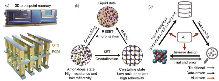
... ,34,38]Commercialized product and working principle of phase-change materials, and artificial intelligence (AI)-driven materials discovery
(a) 3D crosspoint memory[3] (b) principle of phase-change materials[34] (c) AI-driven materials discovery[38] ...
... (a) 3D crosspoint memory[3] (b) principle of phase-change materials[34] (c) AI-driven materials discovery[38] ...
The high-throughput highway to computational materials design
1
2013
... 随着材料基因工程的推进,以高性能材料计算软件与平台、AI技术为驱动的科学研究(AI for science)大幅优化了新材料开发的流程与成本[35~39].材料基因工程旨在通过高通量计算来构建材料数据库,并采用数据驱动的方法来克服材料研发中遇到的挑战[39,40].AI与材料基因工程的深度融合推动了新材料研发方式的革新,由传统的实验“试错法”转变为材料基因工程框架下集高通量筛选、材料基因组数据挖掘与构建、材料反向设计为一体的AI驱动的科学研究范式(图1c[38]),在高熵合金[41,42]、磁性拓扑材料[43,44]、热电材料[45]、塑性层状半导体材料[46,47]等先进材料领域得到了广泛应用.目前,基于密度泛函理论(density functional theory,DFT)计算的材料数据库、高通量自动化智能计算软件等平台发展迅速,如Materials Project[48]、AFLOW[49]和ALKEMIE[50]等,为新材料探索发现带来了极大便利.研究人员可根据不同应用需求,有针对性地筛选与挖掘具有特定属性的材料,并根据计算结果开展进一步的实验制备与验证,大幅缩短了新材料的研发周期. ...
Machine learning for materials research and development
0
2021
机器学习在材料研发中的应用
0
2021
Machine-learned potentials for next-generation matter simulations
4
2021
... 机器学习势的具体拟合过程如图7a[97]所示,主要包括3大步骤:参考数据库的建立、原子环境量化和势能面拟合.依据拟合目标建立全面而精准的数据库是机器学习势的基础.数据库中的参考结构需要具有代表性,不仅能够特征化描述势能面上能量极小值点的结构,还要包含高能量的结构信息,以通过有限数量的原子构型实现对势能面的充分采样.常见的参考数据库来源包括Materials Project[48]、ICSD[115]等材料数据库,AIMD模拟计算,势能迭代训练过程中的结构,以及从头算随机晶体结构搜索(ab initio random structure searching,AIRSS)[116]等.数据库中的结构需要通过DFT进行精确的计算来获取体系中原子的能量和受力信息.完成数据采集后,如何将数据库中体系的空间构型转化为机器学习可识别的数据集,即采用数学表达方式量化原子环境,是下一个核心的问题.该量化指标被称为材料描述符,可以提炼原子局部环境的关键信息,便于高效重构原子环境.一般情况下,某一原子环境的描述符以该原子为中心,将指定截断半径内近邻原子的信息编码,且需要在满足平移、旋转、置换等空间不变性的前提下兼顾计算效率与连贯性.势能面的拟合则是对构型原子环境与能量受力数据的回归过程,通过不断地回归学习减小目标势能面与DFT数据点之间的差异.MLMD通常使用LAMMPS软件进行计算[117].
Process and method for fitting machine learning interatomic potential
(a) construction process of machine learning interatomic potential, according to Ref.[97] (—process of getting the smooth overlap of atomic positions descriptor, σat—smooth parameter, rcut—specified cutoff, ρi (rcut)—obtained atomic density, q—descriptors, E(q)—energies; the red, blue and yellow spheres represent Ge, Te and Sb atoms, respectively) ...
... (d) schematic of the kernel based Gaussian approximation potential, according to Ref.[37] (Ei —potential energy, αi —regression coefficient, k—SOAP similarity) ...
... 机器学习势的具体拟合过程如图7a[97]所示,主要包括3大步骤:参考数据库的建立、原子环境量化和势能面拟合.依据拟合目标建立全面而精准的数据库是机器学习势的基础.数据库中的参考结构需要具有代表性,不仅能够特征化描述势能面上能量极小值点的结构,还要包含高能量的结构信息,以通过有限数量的原子构型实现对势能面的充分采样.常见的参考数据库来源包括Materials Project[48]、ICSD[115]等材料数据库,AIMD模拟计算,势能迭代训练过程中的结构,以及从头算随机晶体结构搜索(ab initio random structure searching,AIRSS)[116]等.数据库中的结构需要通过DFT进行精确的计算来获取体系中原子的能量和受力信息.完成数据采集后,如何将数据库中体系的空间构型转化为机器学习可识别的数据集,即采用数学表达方式量化原子环境,是下一个核心的问题.该量化指标被称为材料描述符,可以提炼原子局部环境的关键信息,便于高效重构原子环境.一般情况下,某一原子环境的描述符以该原子为中心,将指定截断半径内近邻原子的信息编码,且需要在满足平移、旋转、置换等空间不变性的前提下兼顾计算效率与连贯性.势能面的拟合则是对构型原子环境与能量受力数据的回归过程,通过不断地回归学习减小目标势能面与DFT数据点之间的差异.MLMD通常使用LAMMPS软件进行计算[117]. ...
AFLOW-XtalFinder: A reliable choice to identify crystalline prototypes
1
2021
... 随着材料基因工程的推进,以高性能材料计算软件与平台、AI技术为驱动的科学研究(AI for science)大幅优化了新材料开发的流程与成本[35~39].材料基因工程旨在通过高通量计算来构建材料数据库,并采用数据驱动的方法来克服材料研发中遇到的挑战[39,40].AI与材料基因工程的深度融合推动了新材料研发方式的革新,由传统的实验“试错法”转变为材料基因工程框架下集高通量筛选、材料基因组数据挖掘与构建、材料反向设计为一体的AI驱动的科学研究范式(图1c[38]),在高熵合金[41,42]、磁性拓扑材料[43,44]、热电材料[45]、塑性层状半导体材料[46,47]等先进材料领域得到了广泛应用.目前,基于密度泛函理论(density functional theory,DFT)计算的材料数据库、高通量自动化智能计算软件等平台发展迅速,如Materials Project[48]、AFLOW[49]和ALKEMIE[50]等,为新材料探索发现带来了极大便利.研究人员可根据不同应用需求,有针对性地筛选与挖掘具有特定属性的材料,并根据计算结果开展进一步的实验制备与验证,大幅缩短了新材料的研发周期. ...
High-throughput automatic integrated material calculations and data management intelligent platform and the application in novel alloys
2
2022
... 随着材料基因工程的推进,以高性能材料计算软件与平台、AI技术为驱动的科学研究(AI for science)大幅优化了新材料开发的流程与成本[35~39].材料基因工程旨在通过高通量计算来构建材料数据库,并采用数据驱动的方法来克服材料研发中遇到的挑战[39,40].AI与材料基因工程的深度融合推动了新材料研发方式的革新,由传统的实验“试错法”转变为材料基因工程框架下集高通量筛选、材料基因组数据挖掘与构建、材料反向设计为一体的AI驱动的科学研究范式(图1c[38]),在高熵合金[41,42]、磁性拓扑材料[43,44]、热电材料[45]、塑性层状半导体材料[46,47]等先进材料领域得到了广泛应用.目前,基于密度泛函理论(density functional theory,DFT)计算的材料数据库、高通量自动化智能计算软件等平台发展迅速,如Materials Project[48]、AFLOW[49]和ALKEMIE[50]等,为新材料探索发现带来了极大便利.研究人员可根据不同应用需求,有针对性地筛选与挖掘具有特定属性的材料,并根据计算结果开展进一步的实验制备与验证,大幅缩短了新材料的研发周期. ...
High speed overwritable phase change optical disk material
1
1987
... 硫族相变材料于19世纪60年代被首次报道,在19世纪90年代被用于可擦写的光存储产品如rewritable CD,DVD,Blu-ray Disc等[51,52].典型的硫族相变材料GST在纳秒级快速结晶过程中形成立方相结构,其中一个子晶格由Te原子占据,另一个子晶格包含随机分布的Ge原子、Sb原子和大量空位[52].其最小结构单元为Ge/Sb原子与Te原子交替形成的四元环,被称为ABAB (A: Ge/Sb, B: Te)环.而GST的非晶缺乏长程有序性且非晶网络结构十分复杂,此外非晶结构随时间延长发生自发弛豫演化,难以通过单一实验研究对其性质机理从微观角度做出解释.基于DFT的第一性原理分子动力学(ab initio molecular dynamics,AIMD)模拟方法能够有效模拟材料动态过程中的微观结构变化,揭示材料结构相变机理.2007年,Caravati等[53]和Akola等[54]分别首次独立报道了GST非晶态的AIMD计算,使用熔融淬火方法获得了非晶锗锑碲(a-GST)和非晶锗碲(a-GeTe)模型,模型包括约200个原子.具体而言,先将模型原子位置在超高温下随机化,再降温至材料熔点以上保温约30 ps,模拟其液态结构特性,随后以1012 K/s的速率逐步降温至300 K并保温30 ps,从而获得非晶模型.如图2a[53]所示,模拟得到的a-GST的X射线散射因子S(Q)与实验结果一致,证明AIMD的模拟结果可信[53].AIMD结果表明a-GST中存在着大量以Ge、Te原子为中心的缺陷八面体结构,而且包含大量的四元基环(图2b[53]),其中超过80%为ABAB环[54].该现象与基于同步辐射X射线衍射数据的逆向Monte Carlo模拟(reverse Monte Carlo simulations)得到的结果一致[55].ABAB环与立方相中的主要构成单元相似,被认为是相变材料结晶形核过程的重要结构基元.由于SET过程中产生的Joule热可使局部温度达到300℃以上,但在该温度下ABAB环会快速地断开再重联,需要经过较长的孕育期才能够形成稳定的临界晶核(图2c[56]),导致GST存储器件需要至少10 ns才能完成SET操作[56]. ...
Rapid-phase transitions of GeTe-Sb2Te3 pseudobinary amorphous thin films for an optical disk memory
2
1991
... 硫族相变材料于19世纪60年代被首次报道,在19世纪90年代被用于可擦写的光存储产品如rewritable CD,DVD,Blu-ray Disc等[51,52].典型的硫族相变材料GST在纳秒级快速结晶过程中形成立方相结构,其中一个子晶格由Te原子占据,另一个子晶格包含随机分布的Ge原子、Sb原子和大量空位[52].其最小结构单元为Ge/Sb原子与Te原子交替形成的四元环,被称为ABAB (A: Ge/Sb, B: Te)环.而GST的非晶缺乏长程有序性且非晶网络结构十分复杂,此外非晶结构随时间延长发生自发弛豫演化,难以通过单一实验研究对其性质机理从微观角度做出解释.基于DFT的第一性原理分子动力学(ab initio molecular dynamics,AIMD)模拟方法能够有效模拟材料动态过程中的微观结构变化,揭示材料结构相变机理.2007年,Caravati等[53]和Akola等[54]分别首次独立报道了GST非晶态的AIMD计算,使用熔融淬火方法获得了非晶锗锑碲(a-GST)和非晶锗碲(a-GeTe)模型,模型包括约200个原子.具体而言,先将模型原子位置在超高温下随机化,再降温至材料熔点以上保温约30 ps,模拟其液态结构特性,随后以1012 K/s的速率逐步降温至300 K并保温30 ps,从而获得非晶模型.如图2a[53]所示,模拟得到的a-GST的X射线散射因子S(Q)与实验结果一致,证明AIMD的模拟结果可信[53].AIMD结果表明a-GST中存在着大量以Ge、Te原子为中心的缺陷八面体结构,而且包含大量的四元基环(图2b[53]),其中超过80%为ABAB环[54].该现象与基于同步辐射X射线衍射数据的逆向Monte Carlo模拟(reverse Monte Carlo simulations)得到的结果一致[55].ABAB环与立方相中的主要构成单元相似,被认为是相变材料结晶形核过程的重要结构基元.由于SET过程中产生的Joule热可使局部温度达到300℃以上,但在该温度下ABAB环会快速地断开再重联,需要经过较长的孕育期才能够形成稳定的临界晶核(图2c[56]),导致GST存储器件需要至少10 ns才能完成SET操作[56]. ...
... [52].其最小结构单元为Ge/Sb原子与Te原子交替形成的四元环,被称为ABAB (A: Ge/Sb, B: Te)环.而GST的非晶缺乏长程有序性且非晶网络结构十分复杂,此外非晶结构随时间延长发生自发弛豫演化,难以通过单一实验研究对其性质机理从微观角度做出解释.基于DFT的第一性原理分子动力学(ab initio molecular dynamics,AIMD)模拟方法能够有效模拟材料动态过程中的微观结构变化,揭示材料结构相变机理.2007年,Caravati等[53]和Akola等[54]分别首次独立报道了GST非晶态的AIMD计算,使用熔融淬火方法获得了非晶锗锑碲(a-GST)和非晶锗碲(a-GeTe)模型,模型包括约200个原子.具体而言,先将模型原子位置在超高温下随机化,再降温至材料熔点以上保温约30 ps,模拟其液态结构特性,随后以1012 K/s的速率逐步降温至300 K并保温30 ps,从而获得非晶模型.如图2a[53]所示,模拟得到的a-GST的X射线散射因子S(Q)与实验结果一致,证明AIMD的模拟结果可信[53].AIMD结果表明a-GST中存在着大量以Ge、Te原子为中心的缺陷八面体结构,而且包含大量的四元基环(图2b[53]),其中超过80%为ABAB环[54].该现象与基于同步辐射X射线衍射数据的逆向Monte Carlo模拟(reverse Monte Carlo simulations)得到的结果一致[55].ABAB环与立方相中的主要构成单元相似,被认为是相变材料结晶形核过程的重要结构基元.由于SET过程中产生的Joule热可使局部温度达到300℃以上,但在该温度下ABAB环会快速地断开再重联,需要经过较长的孕育期才能够形成稳定的临界晶核(图2c[56]),导致GST存储器件需要至少10 ns才能完成SET操作[56]. ...
Coexistence of tetrahedral- and octahedral-like sites in amorphous phase change materials
6
2007
... 硫族相变材料于19世纪60年代被首次报道,在19世纪90年代被用于可擦写的光存储产品如rewritable CD,DVD,Blu-ray Disc等[51,52].典型的硫族相变材料GST在纳秒级快速结晶过程中形成立方相结构,其中一个子晶格由Te原子占据,另一个子晶格包含随机分布的Ge原子、Sb原子和大量空位[52].其最小结构单元为Ge/Sb原子与Te原子交替形成的四元环,被称为ABAB (A: Ge/Sb, B: Te)环.而GST的非晶缺乏长程有序性且非晶网络结构十分复杂,此外非晶结构随时间延长发生自发弛豫演化,难以通过单一实验研究对其性质机理从微观角度做出解释.基于DFT的第一性原理分子动力学(ab initio molecular dynamics,AIMD)模拟方法能够有效模拟材料动态过程中的微观结构变化,揭示材料结构相变机理.2007年,Caravati等[53]和Akola等[54]分别首次独立报道了GST非晶态的AIMD计算,使用熔融淬火方法获得了非晶锗锑碲(a-GST)和非晶锗碲(a-GeTe)模型,模型包括约200个原子.具体而言,先将模型原子位置在超高温下随机化,再降温至材料熔点以上保温约30 ps,模拟其液态结构特性,随后以1012 K/s的速率逐步降温至300 K并保温30 ps,从而获得非晶模型.如图2a[53]所示,模拟得到的a-GST的X射线散射因子S(Q)与实验结果一致,证明AIMD的模拟结果可信[53].AIMD结果表明a-GST中存在着大量以Ge、Te原子为中心的缺陷八面体结构,而且包含大量的四元基环(图2b[53]),其中超过80%为ABAB环[54].该现象与基于同步辐射X射线衍射数据的逆向Monte Carlo模拟(reverse Monte Carlo simulations)得到的结果一致[55].ABAB环与立方相中的主要构成单元相似,被认为是相变材料结晶形核过程的重要结构基元.由于SET过程中产生的Joule热可使局部温度达到300℃以上,但在该温度下ABAB环会快速地断开再重联,需要经过较长的孕育期才能够形成稳定的临界晶核(图2c[56]),导致GST存储器件需要至少10 ns才能完成SET操作[56]. ...
... [53]所示,模拟得到的a-GST的X射线散射因子S(Q)与实验结果一致,证明AIMD的模拟结果可信[53].AIMD结果表明a-GST中存在着大量以Ge、Te原子为中心的缺陷八面体结构,而且包含大量的四元基环(图2b[53]),其中超过80%为ABAB环[54].该现象与基于同步辐射X射线衍射数据的逆向Monte Carlo模拟(reverse Monte Carlo simulations)得到的结果一致[55].ABAB环与立方相中的主要构成单元相似,被认为是相变材料结晶形核过程的重要结构基元.由于SET过程中产生的Joule热可使局部温度达到300℃以上,但在该温度下ABAB环会快速地断开再重联,需要经过较长的孕育期才能够形成稳定的临界晶核(图2c[56]),导致GST存储器件需要至少10 ns才能完成SET操作[56]. ...
... [53].AIMD结果表明a-GST中存在着大量以Ge、Te原子为中心的缺陷八面体结构,而且包含大量的四元基环(图2b[53]),其中超过80%为ABAB环[54].该现象与基于同步辐射X射线衍射数据的逆向Monte Carlo模拟(reverse Monte Carlo simulations)得到的结果一致[55].ABAB环与立方相中的主要构成单元相似,被认为是相变材料结晶形核过程的重要结构基元.由于SET过程中产生的Joule热可使局部温度达到300℃以上,但在该温度下ABAB环会快速地断开再重联,需要经过较长的孕育期才能够形成稳定的临界晶核(图2c[56]),导致GST存储器件需要至少10 ns才能完成SET操作[56]. ...
... [53]),其中超过80%为ABAB环[54].该现象与基于同步辐射X射线衍射数据的逆向Monte Carlo模拟(reverse Monte Carlo simulations)得到的结果一致[55].ABAB环与立方相中的主要构成单元相似,被认为是相变材料结晶形核过程的重要结构基元.由于SET过程中产生的Joule热可使局部温度达到300℃以上,但在该温度下ABAB环会快速地断开再重联,需要经过较长的孕育期才能够形成稳定的临界晶核(图2c[56]),导致GST存储器件需要至少10 ns才能完成SET操作[56]. ...
... [53,56]<i>Ab initio</i> molecular dynamic (AIMD) modeling of amorphous Ge<sub>2</sub>Sb<sub>2</sub>Te<sub>5</sub> phase-change material (a, b) structure factor (a) and ring lengths (b) distribution calculated at 300 K<sup>[<xref ref-type="bibr" rid="R53">53</xref>]</sup> ( <strong><i>Q</i></strong> —scattering vector, <i>S</i>( <strong><i>Q</i></strong> )—X-ray scattering factor, a-GST—amorphous GST, <i>ABAB</i>—<i>ABAB</i> rings, <i>A</i>: Ge/Sb, <i>B</i>: Te) (c) evolution of <i>ABAB</i> rings calculated at about 600 K<sup>[<xref ref-type="bibr" rid="R56">56</xref>]</sup>Fig.2
Structural phase transitions on the nanoscale: The crucial pattern in the phase-change materials Ge2Sb2Te5 and GeTe
2
2007
... 硫族相变材料于19世纪60年代被首次报道,在19世纪90年代被用于可擦写的光存储产品如rewritable CD,DVD,Blu-ray Disc等[51,52].典型的硫族相变材料GST在纳秒级快速结晶过程中形成立方相结构,其中一个子晶格由Te原子占据,另一个子晶格包含随机分布的Ge原子、Sb原子和大量空位[52].其最小结构单元为Ge/Sb原子与Te原子交替形成的四元环,被称为ABAB (A: Ge/Sb, B: Te)环.而GST的非晶缺乏长程有序性且非晶网络结构十分复杂,此外非晶结构随时间延长发生自发弛豫演化,难以通过单一实验研究对其性质机理从微观角度做出解释.基于DFT的第一性原理分子动力学(ab initio molecular dynamics,AIMD)模拟方法能够有效模拟材料动态过程中的微观结构变化,揭示材料结构相变机理.2007年,Caravati等[53]和Akola等[54]分别首次独立报道了GST非晶态的AIMD计算,使用熔融淬火方法获得了非晶锗锑碲(a-GST)和非晶锗碲(a-GeTe)模型,模型包括约200个原子.具体而言,先将模型原子位置在超高温下随机化,再降温至材料熔点以上保温约30 ps,模拟其液态结构特性,随后以1012 K/s的速率逐步降温至300 K并保温30 ps,从而获得非晶模型.如图2a[53]所示,模拟得到的a-GST的X射线散射因子S(Q)与实验结果一致,证明AIMD的模拟结果可信[53].AIMD结果表明a-GST中存在着大量以Ge、Te原子为中心的缺陷八面体结构,而且包含大量的四元基环(图2b[53]),其中超过80%为ABAB环[54].该现象与基于同步辐射X射线衍射数据的逆向Monte Carlo模拟(reverse Monte Carlo simulations)得到的结果一致[55].ABAB环与立方相中的主要构成单元相似,被认为是相变材料结晶形核过程的重要结构基元.由于SET过程中产生的Joule热可使局部温度达到300℃以上,但在该温度下ABAB环会快速地断开再重联,需要经过较长的孕育期才能够形成稳定的临界晶核(图2c[56]),导致GST存储器件需要至少10 ns才能完成SET操作[56]. ...
... [54].该现象与基于同步辐射X射线衍射数据的逆向Monte Carlo模拟(reverse Monte Carlo simulations)得到的结果一致[55].ABAB环与立方相中的主要构成单元相似,被认为是相变材料结晶形核过程的重要结构基元.由于SET过程中产生的Joule热可使局部温度达到300℃以上,但在该温度下ABAB环会快速地断开再重联,需要经过较长的孕育期才能够形成稳定的临界晶核(图2c[56]),导致GST存储器件需要至少10 ns才能完成SET操作[56]. ...
Structural basis for the fast phase change of Ge2Sb2Te5: Ring statistics analogy between the crystal and amorphous states
1
2006
... 硫族相变材料于19世纪60年代被首次报道,在19世纪90年代被用于可擦写的光存储产品如rewritable CD,DVD,Blu-ray Disc等[51,52].典型的硫族相变材料GST在纳秒级快速结晶过程中形成立方相结构,其中一个子晶格由Te原子占据,另一个子晶格包含随机分布的Ge原子、Sb原子和大量空位[52].其最小结构单元为Ge/Sb原子与Te原子交替形成的四元环,被称为ABAB (A: Ge/Sb, B: Te)环.而GST的非晶缺乏长程有序性且非晶网络结构十分复杂,此外非晶结构随时间延长发生自发弛豫演化,难以通过单一实验研究对其性质机理从微观角度做出解释.基于DFT的第一性原理分子动力学(ab initio molecular dynamics,AIMD)模拟方法能够有效模拟材料动态过程中的微观结构变化,揭示材料结构相变机理.2007年,Caravati等[53]和Akola等[54]分别首次独立报道了GST非晶态的AIMD计算,使用熔融淬火方法获得了非晶锗锑碲(a-GST)和非晶锗碲(a-GeTe)模型,模型包括约200个原子.具体而言,先将模型原子位置在超高温下随机化,再降温至材料熔点以上保温约30 ps,模拟其液态结构特性,随后以1012 K/s的速率逐步降温至300 K并保温30 ps,从而获得非晶模型.如图2a[53]所示,模拟得到的a-GST的X射线散射因子S(Q)与实验结果一致,证明AIMD的模拟结果可信[53].AIMD结果表明a-GST中存在着大量以Ge、Te原子为中心的缺陷八面体结构,而且包含大量的四元基环(图2b[53]),其中超过80%为ABAB环[54].该现象与基于同步辐射X射线衍射数据的逆向Monte Carlo模拟(reverse Monte Carlo simulations)得到的结果一致[55].ABAB环与立方相中的主要构成单元相似,被认为是相变材料结晶形核过程的重要结构基元.由于SET过程中产生的Joule热可使局部温度达到300℃以上,但在该温度下ABAB环会快速地断开再重联,需要经过较长的孕育期才能够形成稳定的临界晶核(图2c[56]),导致GST存储器件需要至少10 ns才能完成SET操作[56]. ...
Reducing the stochasticity of crystal nucleation to enable subnanosecond memory writing
12
2017
... 硫族相变材料于19世纪60年代被首次报道,在19世纪90年代被用于可擦写的光存储产品如rewritable CD,DVD,Blu-ray Disc等[51,52].典型的硫族相变材料GST在纳秒级快速结晶过程中形成立方相结构,其中一个子晶格由Te原子占据,另一个子晶格包含随机分布的Ge原子、Sb原子和大量空位[52].其最小结构单元为Ge/Sb原子与Te原子交替形成的四元环,被称为ABAB (A: Ge/Sb, B: Te)环.而GST的非晶缺乏长程有序性且非晶网络结构十分复杂,此外非晶结构随时间延长发生自发弛豫演化,难以通过单一实验研究对其性质机理从微观角度做出解释.基于DFT的第一性原理分子动力学(ab initio molecular dynamics,AIMD)模拟方法能够有效模拟材料动态过程中的微观结构变化,揭示材料结构相变机理.2007年,Caravati等[53]和Akola等[54]分别首次独立报道了GST非晶态的AIMD计算,使用熔融淬火方法获得了非晶锗锑碲(a-GST)和非晶锗碲(a-GeTe)模型,模型包括约200个原子.具体而言,先将模型原子位置在超高温下随机化,再降温至材料熔点以上保温约30 ps,模拟其液态结构特性,随后以1012 K/s的速率逐步降温至300 K并保温30 ps,从而获得非晶模型.如图2a[53]所示,模拟得到的a-GST的X射线散射因子S(Q)与实验结果一致,证明AIMD的模拟结果可信[53].AIMD结果表明a-GST中存在着大量以Ge、Te原子为中心的缺陷八面体结构,而且包含大量的四元基环(图2b[53]),其中超过80%为ABAB环[54].该现象与基于同步辐射X射线衍射数据的逆向Monte Carlo模拟(reverse Monte Carlo simulations)得到的结果一致[55].ABAB环与立方相中的主要构成单元相似,被认为是相变材料结晶形核过程的重要结构基元.由于SET过程中产生的Joule热可使局部温度达到300℃以上,但在该温度下ABAB环会快速地断开再重联,需要经过较长的孕育期才能够形成稳定的临界晶核(图2c[56]),导致GST存储器件需要至少10 ns才能完成SET操作[56]. ...
... [56]. ...
... ,56]<i>Ab initio</i> molecular dynamic (AIMD) modeling of amorphous Ge<sub>2</sub>Sb<sub>2</sub>Te<sub>5</sub> phase-change material (a, b) structure factor (a) and ring lengths (b) distribution calculated at 300 K<sup>[<xref ref-type="bibr" rid="R53">53</xref>]</sup> ( <strong><i>Q</i></strong> —scattering vector, <i>S</i>( <strong><i>Q</i></strong> )—X-ray scattering factor, a-GST—amorphous GST, <i>ABAB</i>—<i>ABAB</i> rings, <i>A</i>: Ge/Sb, <i>B</i>: Te) (c) evolution of <i>ABAB</i> rings calculated at about 600 K<sup>[<xref ref-type="bibr" rid="R56">56</xref>]</sup>Fig.2
... [56]Design of Sc<sub>0.2</sub>Sb<sub>2</sub>Te<sub>3</sub> phase-change alloy with ultrafast nucleation rate and device validation<sup>[<xref ref-type="bibr" rid="R56">56</xref>]</sup>
(a) structure of rocksalt Sb2Te3 (Ecoh—cohesive energy, a—cell length, the yellow spheres represent the sublattice occupied by Sb atoms and vacancies with a ratio of 2∶1, the blue spheres represent the sublattice occupied by Te atoms) ...
... [56]
(a) structure of rocksalt Sb2Te3 (Ecoh—cohesive energy, a—cell length, the yellow spheres represent the sublattice occupied by Sb atoms and vacancies with a ratio of 2∶1, the blue spheres represent the sublattice occupied by Te atoms) ...
Characterization of supercooled liquid Ge2Sb2Te5 and its crystallization by ultrafast-heating calorimetry
... [61]AIMD crystallization simulations of a 1008-atom Ge<sub>1</sub>Sb<sub>2</sub>Te<sub>4</sub> model at about 600 K<sup>[<xref ref-type="bibr" rid="R61">61</xref>]</sup>
(a) snapshots of the crystallization process identified by ...
... [61]
(a) snapshots of the crystallization process identified by ...
... 机器学习势的具体拟合过程如图7a[97]所示,主要包括3大步骤:参考数据库的建立、原子环境量化和势能面拟合.依据拟合目标建立全面而精准的数据库是机器学习势的基础.数据库中的参考结构需要具有代表性,不仅能够特征化描述势能面上能量极小值点的结构,还要包含高能量的结构信息,以通过有限数量的原子构型实现对势能面的充分采样.常见的参考数据库来源包括Materials Project[48]、ICSD[115]等材料数据库,AIMD模拟计算,势能迭代训练过程中的结构,以及从头算随机晶体结构搜索(ab initio random structure searching,AIRSS)[116]等.数据库中的结构需要通过DFT进行精确的计算来获取体系中原子的能量和受力信息.完成数据采集后,如何将数据库中体系的空间构型转化为机器学习可识别的数据集,即采用数学表达方式量化原子环境,是下一个核心的问题.该量化指标被称为材料描述符,可以提炼原子局部环境的关键信息,便于高效重构原子环境.一般情况下,某一原子环境的描述符以该原子为中心,将指定截断半径内近邻原子的信息编码,且需要在满足平移、旋转、置换等空间不变性的前提下兼顾计算效率与连贯性.势能面的拟合则是对构型原子环境与能量受力数据的回归过程,通过不断地回归学习减小目标势能面与DFT数据点之间的差异.MLMD通常使用LAMMPS软件进行计算[117]. ...
... ,97,118,119]得到的机器学习原子间势的拟合过程及方法Process and method for fitting machine learning interatomic potential
(a) construction process of machine learning interatomic potential, according to Ref.[97] (—process of getting the smooth overlap of atomic positions descriptor, σat—smooth parameter, rcut—specified cutoff, ρi (rcut)—obtained atomic density, q—descriptors, E(q)—energies; the red, blue and yellow spheres represent Ge, Te and Sb atoms, respectively) ...
... (a) construction process of machine learning interatomic potential, according to Ref.[97] (—process of getting the smooth overlap of atomic positions descriptor, σat—smooth parameter, rcut—specified cutoff, ρi (rcut)—obtained atomic density, q—descriptors, E(q)—energies; the red, blue and yellow spheres represent Ge, Te and Sb atoms, respectively) ...
DeePMD-kit: A deep learning package for many-body potential energy representation and molecular dynamics
0
2018
Machine learning interatomic potential: Bridge the gap between small-scale models and realistic device-scale simulations
1
2024
... 如上所述,由于第一性原理分子动力学模拟的模型尺寸与计算成本限制,无法在保证量子力学计算精度的同时满足器件尺度计算的需求,难以预测评估相变材料在实际应用中的表现.尽管单一计算工具很难实现从微观尺度材料结构到宏观尺度器件应用上的仿真,但是先进仿真模拟软件提供了多场耦合表征宏观性能的手段.一方面,通过参数传递,如将微观的DFT计算结果与有限元(finite element method,FEM)、时域有限差分(finite-difference time-domain,FDTD)等仿真方法进行耦合,可实现材料在器件尺度下宏观性质的模拟,并为器件应用提供理论指导[94~96],该方式可称为“多尺度模拟”.另一方面,近年来基于机器学习势函数的分子动力学方法(machine learning molecular dynamics,MLMD)能够在保持量子力学计算精度的前提下,跨越传统AIMD计算中时间尺度与空间尺度的局限性[97~99],实现器件尺度的原子计算,进而辅助相变存储器件设计[100],该类计算工作可称为“跨尺度模拟”. ...
Device-scale atomistic modelling of phase-change memory materials
11
2023
... 如上所述,由于第一性原理分子动力学模拟的模型尺寸与计算成本限制,无法在保证量子力学计算精度的同时满足器件尺度计算的需求,难以预测评估相变材料在实际应用中的表现.尽管单一计算工具很难实现从微观尺度材料结构到宏观尺度器件应用上的仿真,但是先进仿真模拟软件提供了多场耦合表征宏观性能的手段.一方面,通过参数传递,如将微观的DFT计算结果与有限元(finite element method,FEM)、时域有限差分(finite-difference time-domain,FDTD)等仿真方法进行耦合,可实现材料在器件尺度下宏观性质的模拟,并为器件应用提供理论指导[94~96],该方式可称为“多尺度模拟”.另一方面,近年来基于机器学习势函数的分子动力学方法(machine learning molecular dynamics,MLMD)能够在保持量子力学计算精度的前提下,跨越传统AIMD计算中时间尺度与空间尺度的局限性[97~99],实现器件尺度的原子计算,进而辅助相变存储器件设计[100],该类计算工作可称为“跨尺度模拟”. ...
Multiscale simulation of Sb<sub>2</sub>Te<sub>1</sub> phase change alloy for waveguide devices <sup>[<xref ref-type="bibr" rid="R111">111</xref>]</sup>
(a) local structural snapshots of amorphous and crystalline Sb2Te1 (amor.—amorphous; crys.—crystalline; Sb and Te atoms are rendered as yellow and green spheres, respectively) ...
... [111]
(a) local structural snapshots of amorphous and crystalline Sb2Te1 (amor.—amorphous; crys.—crystalline; Sb and Te atoms are rendered as yellow and green spheres, respectively) ...
... Wang等[111]将DFT计算得到的Sb2Te1的光学性质作为关键参数传递至FDTD仿真软件Lumerical[113]并进行了光学器件模拟.硅光技术的快速发展为PCM光子器件的大规模集成带来了新的契机.图6c[111]给出了典型的PCM光波导器件,该器件由SiO2绝缘体、绝缘体上硅波导(silicon-on-insulator,SOI)、沉积在硅波导上的相变薄膜与氧化铟锡(indium tin oxide,ITO)覆盖层构成.入射光信号沿着硅波导传播时会与相变薄膜之间发生倏逝耦合形成倏逝场,由于相变薄膜在不同相态下具有不同的消光系数,入射光未能被全反射的部分被不同程度地吸收.当入射光强度较大时,相变材料吸收能量产生的Joule热足以诱发材料相变,完成对信息的编码;当入射光强度适中时,材料的相态不会发生改变,通过测量经过相变薄膜区域后出射光的光强度便可完成对信息的读取.图6d[111]给出了长度为2与1 μm的Sb2Te1波导器件光透过率的FDTD仿真结果,在长度为1 μm器件中透过率对比窗口最大可达40%,超越了Ge-Sb-Te光波导器件约20%[28].图6e[111]分别对应了Sb2Te1合金3种结构的电场|E|分布图,直观地展示了处于不同相态的波导器件的光透过程度.需注意的是,当Sb2Te1的透射率差异最大时,晶体相为无序菱方结构,而Te有序化会减小该窗口,即额外的升温退火处理会减弱Sb2Te1波导器件的性能.因此,在使用该类器件时应当进行高频高速的器件操作,并且降低环境温度的干扰.该工作是多尺度模拟指导PCM光学应用研究的典型案例.近期,Zheng等[114]通过原位电子显微学实验,报道了Sb2Te1存在无序菱方亚稳相以及其向稳定有序A7层状结构转变的微观演化过程,证实了Wang等[111]AIMD的计算结果. ...
... [111]给出了典型的PCM光波导器件,该器件由SiO2绝缘体、绝缘体上硅波导(silicon-on-insulator,SOI)、沉积在硅波导上的相变薄膜与氧化铟锡(indium tin oxide,ITO)覆盖层构成.入射光信号沿着硅波导传播时会与相变薄膜之间发生倏逝耦合形成倏逝场,由于相变薄膜在不同相态下具有不同的消光系数,入射光未能被全反射的部分被不同程度地吸收.当入射光强度较大时,相变材料吸收能量产生的Joule热足以诱发材料相变,完成对信息的编码;当入射光强度适中时,材料的相态不会发生改变,通过测量经过相变薄膜区域后出射光的光强度便可完成对信息的读取.图6d[111]给出了长度为2与1 μm的Sb2Te1波导器件光透过率的FDTD仿真结果,在长度为1 μm器件中透过率对比窗口最大可达40%,超越了Ge-Sb-Te光波导器件约20%[28].图6e[111]分别对应了Sb2Te1合金3种结构的电场|E|分布图,直观地展示了处于不同相态的波导器件的光透过程度.需注意的是,当Sb2Te1的透射率差异最大时,晶体相为无序菱方结构,而Te有序化会减小该窗口,即额外的升温退火处理会减弱Sb2Te1波导器件的性能.因此,在使用该类器件时应当进行高频高速的器件操作,并且降低环境温度的干扰.该工作是多尺度模拟指导PCM光学应用研究的典型案例.近期,Zheng等[114]通过原位电子显微学实验,报道了Sb2Te1存在无序菱方亚稳相以及其向稳定有序A7层状结构转变的微观演化过程,证实了Wang等[111]AIMD的计算结果. ...
... Wang等[111]将DFT计算得到的Sb2Te1的光学性质作为关键参数传递至FDTD仿真软件Lumerical[113]并进行了光学器件模拟.硅光技术的快速发展为PCM光子器件的大规模集成带来了新的契机.图6c[111]给出了典型的PCM光波导器件,该器件由SiO2绝缘体、绝缘体上硅波导(silicon-on-insulator,SOI)、沉积在硅波导上的相变薄膜与氧化铟锡(indium tin oxide,ITO)覆盖层构成.入射光信号沿着硅波导传播时会与相变薄膜之间发生倏逝耦合形成倏逝场,由于相变薄膜在不同相态下具有不同的消光系数,入射光未能被全反射的部分被不同程度地吸收.当入射光强度较大时,相变材料吸收能量产生的Joule热足以诱发材料相变,完成对信息的编码;当入射光强度适中时,材料的相态不会发生改变,通过测量经过相变薄膜区域后出射光的光强度便可完成对信息的读取.图6d[111]给出了长度为2与1 μm的Sb2Te1波导器件光透过率的FDTD仿真结果,在长度为1 μm器件中透过率对比窗口最大可达40%,超越了Ge-Sb-Te光波导器件约20%[28].图6e[111]分别对应了Sb2Te1合金3种结构的电场|E|分布图,直观地展示了处于不同相态的波导器件的光透过程度.需注意的是,当Sb2Te1的透射率差异最大时,晶体相为无序菱方结构,而Te有序化会减小该窗口,即额外的升温退火处理会减弱Sb2Te1波导器件的性能.因此,在使用该类器件时应当进行高频高速的器件操作,并且降低环境温度的干扰.该工作是多尺度模拟指导PCM光学应用研究的典型案例.近期,Zheng等[114]通过原位电子显微学实验,报道了Sb2Te1存在无序菱方亚稳相以及其向稳定有序A7层状结构转变的微观演化过程,证实了Wang等[111]AIMD的计算结果. ...
A complicated route from disorder to order in antimony-tellurium binary phase change materials
1
2024
... Wang等[111]将DFT计算得到的Sb2Te1的光学性质作为关键参数传递至FDTD仿真软件Lumerical[113]并进行了光学器件模拟.硅光技术的快速发展为PCM光子器件的大规模集成带来了新的契机.图6c[111]给出了典型的PCM光波导器件,该器件由SiO2绝缘体、绝缘体上硅波导(silicon-on-insulator,SOI)、沉积在硅波导上的相变薄膜与氧化铟锡(indium tin oxide,ITO)覆盖层构成.入射光信号沿着硅波导传播时会与相变薄膜之间发生倏逝耦合形成倏逝场,由于相变薄膜在不同相态下具有不同的消光系数,入射光未能被全反射的部分被不同程度地吸收.当入射光强度较大时,相变材料吸收能量产生的Joule热足以诱发材料相变,完成对信息的编码;当入射光强度适中时,材料的相态不会发生改变,通过测量经过相变薄膜区域后出射光的光强度便可完成对信息的读取.图6d[111]给出了长度为2与1 μm的Sb2Te1波导器件光透过率的FDTD仿真结果,在长度为1 μm器件中透过率对比窗口最大可达40%,超越了Ge-Sb-Te光波导器件约20%[28].图6e[111]分别对应了Sb2Te1合金3种结构的电场|E|分布图,直观地展示了处于不同相态的波导器件的光透过程度.需注意的是,当Sb2Te1的透射率差异最大时,晶体相为无序菱方结构,而Te有序化会减小该窗口,即额外的升温退火处理会减弱Sb2Te1波导器件的性能.因此,在使用该类器件时应当进行高频高速的器件操作,并且降低环境温度的干扰.该工作是多尺度模拟指导PCM光学应用研究的典型案例.近期,Zheng等[114]通过原位电子显微学实验,报道了Sb2Te1存在无序菱方亚稳相以及其向稳定有序A7层状结构转变的微观演化过程,证实了Wang等[111]AIMD的计算结果. ...
New developments in the Inorganic Crystal Structure Database (ICSD): Accessibility in support of materials research and design
1
2002
... 机器学习势的具体拟合过程如图7a[97]所示,主要包括3大步骤:参考数据库的建立、原子环境量化和势能面拟合.依据拟合目标建立全面而精准的数据库是机器学习势的基础.数据库中的参考结构需要具有代表性,不仅能够特征化描述势能面上能量极小值点的结构,还要包含高能量的结构信息,以通过有限数量的原子构型实现对势能面的充分采样.常见的参考数据库来源包括Materials Project[48]、ICSD[115]等材料数据库,AIMD模拟计算,势能迭代训练过程中的结构,以及从头算随机晶体结构搜索(ab initio random structure searching,AIRSS)[116]等.数据库中的结构需要通过DFT进行精确的计算来获取体系中原子的能量和受力信息.完成数据采集后,如何将数据库中体系的空间构型转化为机器学习可识别的数据集,即采用数学表达方式量化原子环境,是下一个核心的问题.该量化指标被称为材料描述符,可以提炼原子局部环境的关键信息,便于高效重构原子环境.一般情况下,某一原子环境的描述符以该原子为中心,将指定截断半径内近邻原子的信息编码,且需要在满足平移、旋转、置换等空间不变性的前提下兼顾计算效率与连贯性.势能面的拟合则是对构型原子环境与能量受力数据的回归过程,通过不断地回归学习减小目标势能面与DFT数据点之间的差异.MLMD通常使用LAMMPS软件进行计算[117]. ...
Ab initio random structure searching
1
2011
... 机器学习势的具体拟合过程如图7a[97]所示,主要包括3大步骤:参考数据库的建立、原子环境量化和势能面拟合.依据拟合目标建立全面而精准的数据库是机器学习势的基础.数据库中的参考结构需要具有代表性,不仅能够特征化描述势能面上能量极小值点的结构,还要包含高能量的结构信息,以通过有限数量的原子构型实现对势能面的充分采样.常见的参考数据库来源包括Materials Project[48]、ICSD[115]等材料数据库,AIMD模拟计算,势能迭代训练过程中的结构,以及从头算随机晶体结构搜索(ab initio random structure searching,AIRSS)[116]等.数据库中的结构需要通过DFT进行精确的计算来获取体系中原子的能量和受力信息.完成数据采集后,如何将数据库中体系的空间构型转化为机器学习可识别的数据集,即采用数学表达方式量化原子环境,是下一个核心的问题.该量化指标被称为材料描述符,可以提炼原子局部环境的关键信息,便于高效重构原子环境.一般情况下,某一原子环境的描述符以该原子为中心,将指定截断半径内近邻原子的信息编码,且需要在满足平移、旋转、置换等空间不变性的前提下兼顾计算效率与连贯性.势能面的拟合则是对构型原子环境与能量受力数据的回归过程,通过不断地回归学习减小目标势能面与DFT数据点之间的差异.MLMD通常使用LAMMPS软件进行计算[117]. ...
LAMMPS—A flexible simulation tool for particle-based materials modeling at the atomic, meso, and continuum scales
1
2022
... 机器学习势的具体拟合过程如图7a[97]所示,主要包括3大步骤:参考数据库的建立、原子环境量化和势能面拟合.依据拟合目标建立全面而精准的数据库是机器学习势的基础.数据库中的参考结构需要具有代表性,不仅能够特征化描述势能面上能量极小值点的结构,还要包含高能量的结构信息,以通过有限数量的原子构型实现对势能面的充分采样.常见的参考数据库来源包括Materials Project[48]、ICSD[115]等材料数据库,AIMD模拟计算,势能迭代训练过程中的结构,以及从头算随机晶体结构搜索(ab initio random structure searching,AIRSS)[116]等.数据库中的结构需要通过DFT进行精确的计算来获取体系中原子的能量和受力信息.完成数据采集后,如何将数据库中体系的空间构型转化为机器学习可识别的数据集,即采用数学表达方式量化原子环境,是下一个核心的问题.该量化指标被称为材料描述符,可以提炼原子局部环境的关键信息,便于高效重构原子环境.一般情况下,某一原子环境的描述符以该原子为中心,将指定截断半径内近邻原子的信息编码,且需要在满足平移、旋转、置换等空间不变性的前提下兼顾计算效率与连贯性.势能面的拟合则是对构型原子环境与能量受力数据的回归过程,通过不断地回归学习减小目标势能面与DFT数据点之间的差异.MLMD通常使用LAMMPS软件进行计算[117]. ...
First principles neural network potentials for reactive simulations of large molecular and condensed systems
5
2017
... 机器学习势的具体拟合过程如图7a[97]所示,主要包括3大步骤:参考数据库的建立、原子环境量化和势能面拟合.依据拟合目标建立全面而精准的数据库是机器学习势的基础.数据库中的参考结构需要具有代表性,不仅能够特征化描述势能面上能量极小值点的结构,还要包含高能量的结构信息,以通过有限数量的原子构型实现对势能面的充分采样.常见的参考数据库来源包括Materials Project[48]、ICSD[115]等材料数据库,AIMD模拟计算,势能迭代训练过程中的结构,以及从头算随机晶体结构搜索(ab initio random structure searching,AIRSS)[116]等.数据库中的结构需要通过DFT进行精确的计算来获取体系中原子的能量和受力信息.完成数据采集后,如何将数据库中体系的空间构型转化为机器学习可识别的数据集,即采用数学表达方式量化原子环境,是下一个核心的问题.该量化指标被称为材料描述符,可以提炼原子局部环境的关键信息,便于高效重构原子环境.一般情况下,某一原子环境的描述符以该原子为中心,将指定截断半径内近邻原子的信息编码,且需要在满足平移、旋转、置换等空间不变性的前提下兼顾计算效率与连贯性.势能面的拟合则是对构型原子环境与能量受力数据的回归过程,通过不断地回归学习减小目标势能面与DFT数据点之间的差异.MLMD通常使用LAMMPS软件进行计算[117].
Process and method for fitting machine learning interatomic potential
(a) construction process of machine learning interatomic potential, according to Ref.[97] (—process of getting the smooth overlap of atomic positions descriptor, σat—smooth parameter, rcut—specified cutoff, ρi (rcut)—obtained atomic density, q—descriptors, E(q)—energies; the red, blue and yellow spheres represent Ge, Te and Sb atoms, respectively) ...
... (b) sketch of the neural, networks according to Ref.[118] ( G1, G2—input vectors describing the atomic configurations, —weight sum of the node values, αij —connecting weight parameter, ɛ—potential energy) ...
Crystal graph convolutional neural networks for an accurate and interpretable prediction of material properties
5
2018
... 机器学习势的具体拟合过程如图7a[97]所示,主要包括3大步骤:参考数据库的建立、原子环境量化和势能面拟合.依据拟合目标建立全面而精准的数据库是机器学习势的基础.数据库中的参考结构需要具有代表性,不仅能够特征化描述势能面上能量极小值点的结构,还要包含高能量的结构信息,以通过有限数量的原子构型实现对势能面的充分采样.常见的参考数据库来源包括Materials Project[48]、ICSD[115]等材料数据库,AIMD模拟计算,势能迭代训练过程中的结构,以及从头算随机晶体结构搜索(ab initio random structure searching,AIRSS)[116]等.数据库中的结构需要通过DFT进行精确的计算来获取体系中原子的能量和受力信息.完成数据采集后,如何将数据库中体系的空间构型转化为机器学习可识别的数据集,即采用数学表达方式量化原子环境,是下一个核心的问题.该量化指标被称为材料描述符,可以提炼原子局部环境的关键信息,便于高效重构原子环境.一般情况下,某一原子环境的描述符以该原子为中心,将指定截断半径内近邻原子的信息编码,且需要在满足平移、旋转、置换等空间不变性的前提下兼顾计算效率与连贯性.势能面的拟合则是对构型原子环境与能量受力数据的回归过程,通过不断地回归学习减小目标势能面与DFT数据点之间的差异.MLMD通常使用LAMMPS软件进行计算[117].
Process and method for fitting machine learning interatomic potential
(a) construction process of machine learning interatomic potential, according to Ref.[97] (—process of getting the smooth overlap of atomic positions descriptor, σat—smooth parameter, rcut—specified cutoff, ρi (rcut)—obtained atomic density, q—descriptors, E(q)—energies; the red, blue and yellow spheres represent Ge, Te and Sb atoms, respectively) ...
... (c) schematic of the graph convolutional neural networks[119] ...


