相变存储器材料设计与多尺度模拟的研究进展
Progress on Materials Design and Multiscale Simulations for Phase-Change Memory
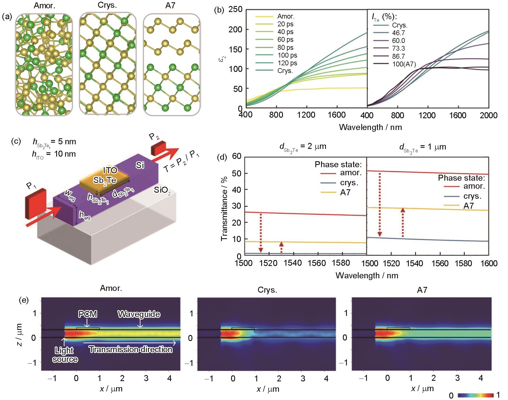
(a) local structural snapshots of amorphous and crystalline Sb2Te1 (amor.—amorphous; crys.—crystalline; Sb and Te atoms are rendered as yellow and green spheres, respectively)
(b) changes in dielectric function upon crystallization and Te ordering (ε2—imaginary part of the dielectric function, ITe—concentration of Te atoms in Te-rich layers)
(c) schematic of a Sb2Te1 waveguide device (ITO—indium tin oxide,
(d) transmittance profiles of different phases
(e) corresponding electric field |E| of the x-z plane of Sb2Te1 device in different phases, the color bar below shows the normalized electric field intensity (PCM—phase-change materials)