PHASE FIELD SIMULATION ON MICROSTRUCTURE EVOLUTION AND GROWTH KINETICS OF Cu6Sn5 INTERMETALLIC COMPOUND DURING EARLY INTERFACIAL REACTION IN Sn/Cu SOLDERING SYSTEM
KE Changbo1, 2, , ZHOU Minbo2, ZHANG Xinping2
1 School of Mechanical and Automotive Engineering, South China University of Technology, Guangzhou 5106402 School of Materials Science and Engineering, South China University of Technology, Guangzhou 510640
中图分类号:
TG113
通讯作者: Correspondent: ZHANG Xinping, professor, Tel: (020)22236396, E-mail: mexzhang@scut.edu.cn
In the continuous pursuit of miniaturization, multifunction and high-reliability of electronic products and devices, the packing density has been increasing and the dimension of solder joints has been scaling down. In electronic packaging, during the soldering process being employed to Sn-based solders, an intermetallic compound (IMC) layer is formed between molten solder and pad (or under bump metallization, UBM), whose morphology and thickness as well as growth kinetics play an important role in controlling the service performance of the solder joints, in particular for solder interconnects with the decreasing size where the interfacial IMC layer takes up a high volume fraction in the solder joint. Thus, characterizing the morphology change and growth kinetics of interfacial IMC layer is very important to optimize the soldering process and evaluate the reliability of solder interconnects. In this study, a multi-phase-field model is applied to intensively account for the effect of grain boundary diffusion coefficient () and IMC/liquid interfacial energy on the morphology evolution and and growth kinetics of IMC. The simulation results show that Cu6Sn5 grains grow up and contact with each other exhibiting a scallop-like morphology which can be influenced by both the grain boundary diffusion coefficient and IMC/liquid interfacial energy. The IMC growth process exhibits three stages, including the initial stage associated with Cu6Sn5 grain broadening followed by the transition stage characterized by scallop shape formation and the last normal growth stage dominated by IMC layer thickening and concurrent Cu6Sn5 grain coarsening. It is also found that the IMC layer thickness increases with grain boundary diffusion coefficient but decreases with IMC/liquid interfacial energy, while the scallop average width decreases with grain boundary diffusion coefficient and increases with IMC/liquid interfacial energy. The relationships between IMC layer thickness/width and reaction time can be well fitted by an exponential growth law, in which the large grain boundary diffusion coefficient combined with (where is the grain boundary energy) can produce precise growth exponent closing to that in the ideal solid-liquid interface reaction.
KEChangbo, ZHOUMinbo, ZHANGXinping. PHASE FIELD SIMULATION ON MICROSTRUCTURE EVOLUTION AND GROWTH KINETICS OF Cu6Sn5 INTERMETALLIC COMPOUND DURING EARLY INTERFACIAL REACTION IN Sn/Cu SOLDERING SYSTEM[J]. 金属学报, 2014, 50(3): 294-304 https://doi.org/10.3724/SP.J.1037.2013.00415
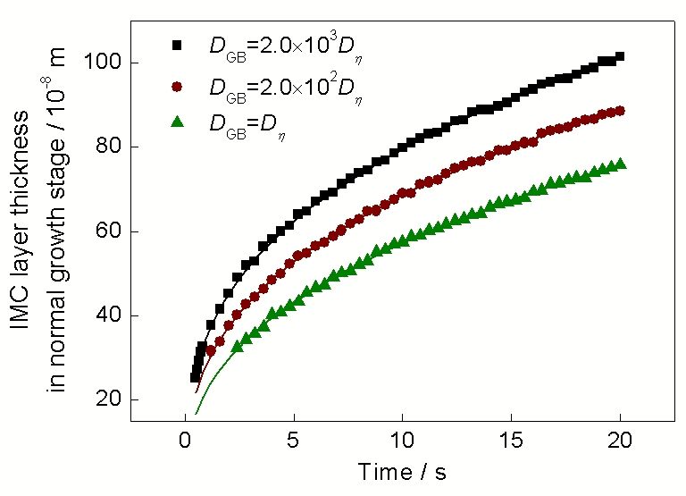
Fig.4 Curves of IMC layer thickness (a) and average width of Cu6Sn5 scallop-type grains (b) vs time for different grain boundary diffusion coefficients
Table 2 Exponential fitting results of variations of IMC layer thickness and average width of Cu6Sn5 scallop-type grains with time during normal growth stage for different grain boundary diffusion coefficients
IMC layer thickness
Scallop average width
R2
KW
nW
R2
2.0×10³Dη
35.44
0.35
0.998
23.16
0.32
0.997
2.0×10²Dη
28.80
0.37
0.997
25.54
0.27
0.991
Dη
22.52
0.40
0.991
16.27
0.48
0.989
Note: KT —growth rate constant, nT —growth exponent, KW—coarsening rate constant, nW—coarsening exponent, R2—square of correlation coefficient
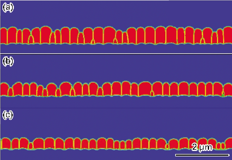
Fig.6 Microstructure of IMC layer with different levels of interfacial energy (t=6 s) (a) =0.08 J/m2 (b) =0.15 J/m2 (c) =0.24 J/m2 (d) the energy balance relationship in triple junction point ( θ is the semi-dihedral angle)
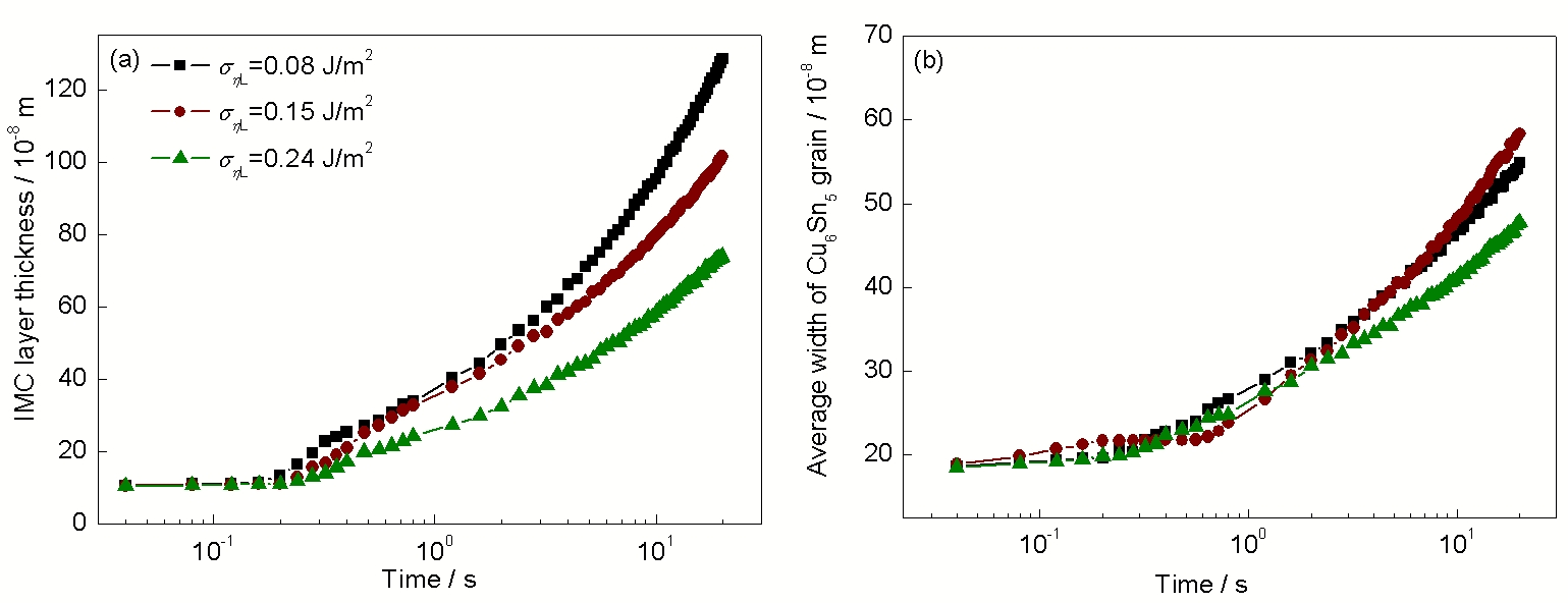
Fig.7 Curves of IMC layer thickness (a) and average width of Cu6Sn5 scallop-type grains (b) vs time for different levels of interfacial energy (DGB=2.0×10³Dη)
Table 3
表3
表3 不同时正常生长阶段IMC层厚度和晶粒横向粒径与时间的指数拟合结果
Table 3 Exponential fitting results of variations of IMC layer thickness and average width of Cu6Sn5 scalloptype grains with time during normal growth stage for different levels of interfacial energy
XuG S,ZengJ B,ZhouM B,CaoS S,MaX,ZhangX P. In: Bi K Y, Yang D G, Cai M eds., Proceedings of the 12th International Conference on Electronic Packaging Technology & High Density Packaging, Piscataway, NJ: IEEE Press, 2012: 289
[26]
ZhouM B, MaX, ZhangX P. Acta Metall Sin, 2013; 3: 341
(周敏波, 马 骁, 张新平. 金属学报, 2013; 3 : 341)
[27]
MaX, WangF J, QianY Y, YoshidaF. Mater Lett, 2003; 57: 3361
[28]
YuD Q, WangL. J Alloys Compd, 2008; 458: 542
[29]
GoshG. J Appl Phys, 2000; 88: 6887
[30]
SuhJ O, TuK N, LutsenkoG V, GusalA M. Acta Mater, 2008; 56: 1075

 , 周敏波
, 周敏波


