Mechanical properties of nanocrystalline materials
1
2005
... 在金属材料内部,当晶粒尺寸减小到纳米级别,相邻晶界(GB)间距也随之降低到纳米尺度,材料强度显著提高[1,2],产生明显的“尺寸效应”[3~8].因此,对于包含丰富界面的纳米材料来说,界面对材料性能的影响将由“辅助作用”变成“主导作用”[5].然而界面在提升材料强度的同时也往往引起应力集中,诱发裂纹,导致材料失效.尤其是在极端应用条件下,界面的快速迁移、辐照缺陷在界面上的富集、界面软化或脆化都会导致材料性能急速下降[9~12].因此,界面调控是获得性能优异的纳米材料的重要途径. ...
Plastic strain localization in metals: Origins and consequences
1
2014
... 在金属材料内部,当晶粒尺寸减小到纳米级别,相邻晶界(GB)间距也随之降低到纳米尺度,材料强度显著提高[1,2],产生明显的“尺寸效应”[3~8].因此,对于包含丰富界面的纳米材料来说,界面对材料性能的影响将由“辅助作用”变成“主导作用”[5].然而界面在提升材料强度的同时也往往引起应力集中,诱发裂纹,导致材料失效.尤其是在极端应用条件下,界面的快速迁移、辐照缺陷在界面上的富集、界面软化或脆化都会导致材料性能急速下降[9~12].因此,界面调控是获得性能优异的纳米材料的重要途径. ...
Length scale-dependent deformation behavior of nanolayered Cu/Zr micropillars
1
2012
... 在金属材料内部,当晶粒尺寸减小到纳米级别,相邻晶界(GB)间距也随之降低到纳米尺度,材料强度显著提高[1,2],产生明显的“尺寸效应”[3~8].因此,对于包含丰富界面的纳米材料来说,界面对材料性能的影响将由“辅助作用”变成“主导作用”[5].然而界面在提升材料强度的同时也往往引起应力集中,诱发裂纹,导致材料失效.尤其是在极端应用条件下,界面的快速迁移、辐照缺陷在界面上的富集、界面软化或脆化都会导致材料性能急速下降[9~12].因此,界面调控是获得性能优异的纳米材料的重要途径. ...
Tailoring nanostructured Cu/Cr multilayer films with enhanced hardness and tunable modulus
0
2012
Achieving optimum mechanical performance in metallic nanolayered Cu/X (X = Zr, Cr) micropillars
1
2014
... 在金属材料内部,当晶粒尺寸减小到纳米级别,相邻晶界(GB)间距也随之降低到纳米尺度,材料强度显著提高[1,2],产生明显的“尺寸效应”[3~8].因此,对于包含丰富界面的纳米材料来说,界面对材料性能的影响将由“辅助作用”变成“主导作用”[5].然而界面在提升材料强度的同时也往往引起应力集中,诱发裂纹,导致材料失效.尤其是在极端应用条件下,界面的快速迁移、辐照缺陷在界面上的富集、界面软化或脆化都会导致材料性能急速下降[9~12].因此,界面调控是获得性能优异的纳米材料的重要途径. ...
Length-scale-dependent cracking and buckling behaviors of nanostructured Cu/Cr multilayer films on compliant substrates
0
2015
Size dependence of buckling strains of Cr films, Cu films and Cu/Cr multilayers on compliant substrates
0
2018
Length-scale-dependent deformation and fracture behavior of Cu/X (X = Nb, Zr) multilayers: The constraining effects of the ductile phase on the brittle phase
1
2011
... 在金属材料内部,当晶粒尺寸减小到纳米级别,相邻晶界(GB)间距也随之降低到纳米尺度,材料强度显著提高[1,2],产生明显的“尺寸效应”[3~8].因此,对于包含丰富界面的纳米材料来说,界面对材料性能的影响将由“辅助作用”变成“主导作用”[5].然而界面在提升材料强度的同时也往往引起应力集中,诱发裂纹,导致材料失效.尤其是在极端应用条件下,界面的快速迁移、辐照缺陷在界面上的富集、界面软化或脆化都会导致材料性能急速下降[9~12].因此,界面调控是获得性能优异的纳米材料的重要途径. ...
Grain growth in nanocrystalline iron prepared by mechanical attrition
1
1997
... 在金属材料内部,当晶粒尺寸减小到纳米级别,相邻晶界(GB)间距也随之降低到纳米尺度,材料强度显著提高[1,2],产生明显的“尺寸效应”[3~8].因此,对于包含丰富界面的纳米材料来说,界面对材料性能的影响将由“辅助作用”变成“主导作用”[5].然而界面在提升材料强度的同时也往往引起应力集中,诱发裂纹,导致材料失效.尤其是在极端应用条件下,界面的快速迁移、辐照缺陷在界面上的富集、界面软化或脆化都会导致材料性能急速下降[9~12].因此,界面调控是获得性能优异的纳米材料的重要途径. ...
Efficient annealing of radiation damage near grain boundaries via interstitial emission
0
2010
Creep resistance of bulk copper-niobium composites: An inverse effect of multilayer length scale
0
2019
Effect of void morphology on void facilitated plasticity in irradiated Cu/Nb metallic nanolayered composites
2
2022
... 在金属材料内部,当晶粒尺寸减小到纳米级别,相邻晶界(GB)间距也随之降低到纳米尺度,材料强度显著提高[1,2],产生明显的“尺寸效应”[3~8].因此,对于包含丰富界面的纳米材料来说,界面对材料性能的影响将由“辅助作用”变成“主导作用”[5].然而界面在提升材料强度的同时也往往引起应力集中,诱发裂纹,导致材料失效.尤其是在极端应用条件下,界面的快速迁移、辐照缺陷在界面上的富集、界面软化或脆化都会导致材料性能急速下降[9~12].因此,界面调控是获得性能优异的纳米材料的重要途径. ...
... 随着层状材料层厚继续减小至几十纳米,层内存储的位错数目已经显著减少,导致位错塞积作用的减弱甚至不能形成塞积,此时Hall-Petch关系不再适用[55,56].Misra等[13]提出约束层滑移机制,来解释在此尺度下的强化机制:作用在位错上的应力不足以使位错穿过界面,单根位错被界面钉扎并沿平行于界面的方向弓出滑移.此时层状材料的屈服应力σcls可以表示为[12]: ...
Length-scale-dependent deformation mechanisms in incoherent metallic multilayered composites
7
2005
... 纳米金属层状材料是由层厚在纳米尺度的不同成分金属交替排列而制成的复合材料.由于这种层状结构可以引入大尺度的平坦界面,使得层状材料常作为研究界面的理想模型材料,为科研人员深入理解界面取向、界面结构和界面成分等界面特征对材料宏观性能的影响提供理论基础.此外,纳米金属层状材料还具有许多出色的性能,如优异的强度[13~16]、热稳定性[15~19]、抗冲击性能[20~22]和抗辐照损伤能力[23~27],使得其在核电、航空航天等领域具有广阔的应用前景.目前纳米金属层状材料的研究体系主要以铜基为主:如Cu/Nb[28,29]、Cu/Ag[30~32]、Cu/Ni[33~36]、Cu/Ta[37]、Cu/Zr[38~40]等.实验上一般利用近热力学平衡法或非热力学平衡法制备层状复合材料,常见如物理气相沉积(PVD)[41~43]、熔炼法[44,45]和累积叠轧(ARB)[46~52]等.高分辨透射电镜(HRTEM)等表征手段是解析界面结构的主要研究方法.但利用HRTEM只能得到原子尺度界面投影和晶体取向,不能直接观察到界面所在平面内的原子结构,因此分子动力学模拟(MD)常作为补充手段为人们提供实验无法直接得到的界面信息与变形机制. ...
... 层状材料力学性能优异,但具有强烈的尺寸效应,组元与层厚的改变会影响层内的位错形核、运动和湮灭,进而影响材料的力学性能.如图1[29,32,38,48]所示,不同组元、不同层厚的层状材料其力学性能表现可能截然不同.关于纳米金属层状材料具有优异力学性能的原因, Misra等[13]系统研究了金属层状材料层厚对力学性能的影响,合理地解释了界面主导的强化行为,并根据不同层厚范围提出了相应的位错机制.此外,目前已知的异质界面主导的强度和塑性变形行为主要有:① 阻碍位错运动;② 促进位错形核;③ 承担剪切塑性流变;④ 调控形变孪晶形核.提高界面的力学性能就可以相应提高材料的力学性能,因此通过界面工程可以设计出具有优异力学性能的金属材料.在界面设计时,具体可以利用几何调控、化学成分调控和多组元调控等手段调整界面结构以实现材料宏观力学性能的提高. ...
... Misra等[13]系统研究了铜基纳米层状材料尺度对力学性能的影响,提出了如图2[13]所示的不同层厚下层状材料强度的位错机制. ...
... [13]所示的不同层厚下层状材料强度的位错机制. ...
... [
13]
Schematic illustration of the dislocation mechanisms in metallic multilayer strength at different length scales (<i>σ</i>—strength, <i>b</i>—Burgers vector)<sup>[<xref ref-type="bibr" rid="R13">13</xref>]</sup>Fig.2![]() <strong>1.1</strong> 位错界面塞积机制
<strong>1.1</strong> 位错界面塞积机制在单层厚度 > 100 nm时,层内本身就储存着大量可动的点阵位错和位错源.在外加应力作用下,位错首先在剪切模量较小的晶体中开动.由于界面对位错的阻碍作用,位错会在界面处产生塞积,并且通过相互协同作用克服界面阻碍导致材料屈服.此时,层状材料的强度和层厚之间符合经典的Hall-Petch关系[53,54].随着 减小,层间储存的位错数目降低,导致位错应力场减弱,从而需要更高的外部载荷驱动位错才能穿过界面,使得材料强化. ...
... [
13]
Fig.2![]() <strong>1.1</strong> 位错界面塞积机制
<strong>1.1</strong> 位错界面塞积机制在单层厚度 > 100 nm时,层内本身就储存着大量可动的点阵位错和位错源.在外加应力作用下,位错首先在剪切模量较小的晶体中开动.由于界面对位错的阻碍作用,位错会在界面处产生塞积,并且通过相互协同作用克服界面阻碍导致材料屈服.此时,层状材料的强度和层厚之间符合经典的Hall-Petch关系[53,54].随着 减小,层间储存的位错数目降低,导致位错应力场减弱,从而需要更高的外部载荷驱动位错才能穿过界面,使得材料强化. ...
... 随着层状材料层厚继续减小至几十纳米,层内存储的位错数目已经显著减少,导致位错塞积作用的减弱甚至不能形成塞积,此时Hall-Petch关系不再适用[55,56].Misra等[13]提出约束层滑移机制,来解释在此尺度下的强化机制:作用在位错上的应力不足以使位错穿过界面,单根位错被界面钉扎并沿平行于界面的方向弓出滑移.此时层状材料的屈服应力σcls可以表示为[12]: ...
Mechanical properties of highly textured Cu/Ni multilayers
0
2011
High-strength and thermally stable bulk nanolayered composites due to twin-induced interfaces
1
2013
... 纳米金属层状材料是由层厚在纳米尺度的不同成分金属交替排列而制成的复合材料.由于这种层状结构可以引入大尺度的平坦界面,使得层状材料常作为研究界面的理想模型材料,为科研人员深入理解界面取向、界面结构和界面成分等界面特征对材料宏观性能的影响提供理论基础.此外,纳米金属层状材料还具有许多出色的性能,如优异的强度[13~16]、热稳定性[15~19]、抗冲击性能[20~22]和抗辐照损伤能力[23~27],使得其在核电、航空航天等领域具有广阔的应用前景.目前纳米金属层状材料的研究体系主要以铜基为主:如Cu/Nb[28,29]、Cu/Ag[30~32]、Cu/Ni[33~36]、Cu/Ta[37]、Cu/Zr[38~40]等.实验上一般利用近热力学平衡法或非热力学平衡法制备层状复合材料,常见如物理气相沉积(PVD)[41~43]、熔炼法[44,45]和累积叠轧(ARB)[46~52]等.高分辨透射电镜(HRTEM)等表征手段是解析界面结构的主要研究方法.但利用HRTEM只能得到原子尺度界面投影和晶体取向,不能直接观察到界面所在平面内的原子结构,因此分子动力学模拟(MD)常作为补充手段为人们提供实验无法直接得到的界面信息与变形机制. ...
High strength and thermal stability of bulk Cu/Ta nanolamellar multilayers fabricated by cross accumulative roll bonding
1
2016
... 纳米金属层状材料是由层厚在纳米尺度的不同成分金属交替排列而制成的复合材料.由于这种层状结构可以引入大尺度的平坦界面,使得层状材料常作为研究界面的理想模型材料,为科研人员深入理解界面取向、界面结构和界面成分等界面特征对材料宏观性能的影响提供理论基础.此外,纳米金属层状材料还具有许多出色的性能,如优异的强度[13~16]、热稳定性[15~19]、抗冲击性能[20~22]和抗辐照损伤能力[23~27],使得其在核电、航空航天等领域具有广阔的应用前景.目前纳米金属层状材料的研究体系主要以铜基为主:如Cu/Nb[28,29]、Cu/Ag[30~32]、Cu/Ni[33~36]、Cu/Ta[37]、Cu/Zr[38~40]等.实验上一般利用近热力学平衡法或非热力学平衡法制备层状复合材料,常见如物理气相沉积(PVD)[41~43]、熔炼法[44,45]和累积叠轧(ARB)[46~52]等.高分辨透射电镜(HRTEM)等表征手段是解析界面结构的主要研究方法.但利用HRTEM只能得到原子尺度界面投影和晶体取向,不能直接观察到界面所在平面内的原子结构,因此分子动力学模拟(MD)常作为补充手段为人们提供实验无法直接得到的界面信息与变形机制. ...
Thermal stability of self-supported nanolayered Cu/Nb films
0
2004
Effects of elevated temperature annealing on the structure and hardness of copper/niobium nanolayered films
0
2005
Thermal stability of Cu-Nb nanolamellar composites fabricated via accumulative roll bonding
1
2013
... 纳米金属层状材料是由层厚在纳米尺度的不同成分金属交替排列而制成的复合材料.由于这种层状结构可以引入大尺度的平坦界面,使得层状材料常作为研究界面的理想模型材料,为科研人员深入理解界面取向、界面结构和界面成分等界面特征对材料宏观性能的影响提供理论基础.此外,纳米金属层状材料还具有许多出色的性能,如优异的强度[13~16]、热稳定性[15~19]、抗冲击性能[20~22]和抗辐照损伤能力[23~27],使得其在核电、航空航天等领域具有广阔的应用前景.目前纳米金属层状材料的研究体系主要以铜基为主:如Cu/Nb[28,29]、Cu/Ag[30~32]、Cu/Ni[33~36]、Cu/Ta[37]、Cu/Zr[38~40]等.实验上一般利用近热力学平衡法或非热力学平衡法制备层状复合材料,常见如物理气相沉积(PVD)[41~43]、熔炼法[44,45]和累积叠轧(ARB)[46~52]等.高分辨透射电镜(HRTEM)等表征手段是解析界面结构的主要研究方法.但利用HRTEM只能得到原子尺度界面投影和晶体取向,不能直接观察到界面所在平面内的原子结构,因此分子动力学模拟(MD)常作为补充手段为人们提供实验无法直接得到的界面信息与变形机制. ...
Deformation and failure of shocked bulk Cu-Nb nanolaminates
1
2014
... 纳米金属层状材料是由层厚在纳米尺度的不同成分金属交替排列而制成的复合材料.由于这种层状结构可以引入大尺度的平坦界面,使得层状材料常作为研究界面的理想模型材料,为科研人员深入理解界面取向、界面结构和界面成分等界面特征对材料宏观性能的影响提供理论基础.此外,纳米金属层状材料还具有许多出色的性能,如优异的强度[13~16]、热稳定性[15~19]、抗冲击性能[20~22]和抗辐照损伤能力[23~27],使得其在核电、航空航天等领域具有广阔的应用前景.目前纳米金属层状材料的研究体系主要以铜基为主:如Cu/Nb[28,29]、Cu/Ag[30~32]、Cu/Ni[33~36]、Cu/Ta[37]、Cu/Zr[38~40]等.实验上一般利用近热力学平衡法或非热力学平衡法制备层状复合材料,常见如物理气相沉积(PVD)[41~43]、熔炼法[44,45]和累积叠轧(ARB)[46~52]等.高分辨透射电镜(HRTEM)等表征手段是解析界面结构的主要研究方法.但利用HRTEM只能得到原子尺度界面投影和晶体取向,不能直接观察到界面所在平面内的原子结构,因此分子动力学模拟(MD)常作为补充手段为人们提供实验无法直接得到的界面信息与变形机制. ...
Layer size effect on the shock compression behavior of fcc-bcc nanolaminates
0
2014
Role of interface structure on the plastic response of Cu/Nb nanolaminates under shock compression: Non-equilibrium molecular dynamics simulations
1
2013
... 纳米金属层状材料是由层厚在纳米尺度的不同成分金属交替排列而制成的复合材料.由于这种层状结构可以引入大尺度的平坦界面,使得层状材料常作为研究界面的理想模型材料,为科研人员深入理解界面取向、界面结构和界面成分等界面特征对材料宏观性能的影响提供理论基础.此外,纳米金属层状材料还具有许多出色的性能,如优异的强度[13~16]、热稳定性[15~19]、抗冲击性能[20~22]和抗辐照损伤能力[23~27],使得其在核电、航空航天等领域具有广阔的应用前景.目前纳米金属层状材料的研究体系主要以铜基为主:如Cu/Nb[28,29]、Cu/Ag[30~32]、Cu/Ni[33~36]、Cu/Ta[37]、Cu/Zr[38~40]等.实验上一般利用近热力学平衡法或非热力学平衡法制备层状复合材料,常见如物理气相沉积(PVD)[41~43]、熔炼法[44,45]和累积叠轧(ARB)[46~52]等.高分辨透射电镜(HRTEM)等表征手段是解析界面结构的主要研究方法.但利用HRTEM只能得到原子尺度界面投影和晶体取向,不能直接观察到界面所在平面内的原子结构,因此分子动力学模拟(MD)常作为补充手段为人们提供实验无法直接得到的界面信息与变形机制. ...
Interface structure and radiation damage resistance in Cu-Nb multilayer nanocomposites
1
2008
... 纳米金属层状材料是由层厚在纳米尺度的不同成分金属交替排列而制成的复合材料.由于这种层状结构可以引入大尺度的平坦界面,使得层状材料常作为研究界面的理想模型材料,为科研人员深入理解界面取向、界面结构和界面成分等界面特征对材料宏观性能的影响提供理论基础.此外,纳米金属层状材料还具有许多出色的性能,如优异的强度[13~16]、热稳定性[15~19]、抗冲击性能[20~22]和抗辐照损伤能力[23~27],使得其在核电、航空航天等领域具有广阔的应用前景.目前纳米金属层状材料的研究体系主要以铜基为主:如Cu/Nb[28,29]、Cu/Ag[30~32]、Cu/Ni[33~36]、Cu/Ta[37]、Cu/Zr[38~40]等.实验上一般利用近热力学平衡法或非热力学平衡法制备层状复合材料,常见如物理气相沉积(PVD)[41~43]、熔炼法[44,45]和累积叠轧(ARB)[46~52]等.高分辨透射电镜(HRTEM)等表征手段是解析界面结构的主要研究方法.但利用HRTEM只能得到原子尺度界面投影和晶体取向,不能直接观察到界面所在平面内的原子结构,因此分子动力学模拟(MD)常作为补充手段为人们提供实验无法直接得到的界面信息与变形机制. ...
Atomic-scale design of radiation-tolerant nanocomposites
0
2010
Radiation damage tolerant nanomaterials
0
2013
Superior tolerance of Ag/Ni multilayers against Kr ion irradiation: An in situ study
0
2013
Stable storage of helium in nanoscale platelets at semicoherent interfaces
1
2013
... 纳米金属层状材料是由层厚在纳米尺度的不同成分金属交替排列而制成的复合材料.由于这种层状结构可以引入大尺度的平坦界面,使得层状材料常作为研究界面的理想模型材料,为科研人员深入理解界面取向、界面结构和界面成分等界面特征对材料宏观性能的影响提供理论基础.此外,纳米金属层状材料还具有许多出色的性能,如优异的强度[13~16]、热稳定性[15~19]、抗冲击性能[20~22]和抗辐照损伤能力[23~27],使得其在核电、航空航天等领域具有广阔的应用前景.目前纳米金属层状材料的研究体系主要以铜基为主:如Cu/Nb[28,29]、Cu/Ag[30~32]、Cu/Ni[33~36]、Cu/Ta[37]、Cu/Zr[38~40]等.实验上一般利用近热力学平衡法或非热力学平衡法制备层状复合材料,常见如物理气相沉积(PVD)[41~43]、熔炼法[44,45]和累积叠轧(ARB)[46~52]等.高分辨透射电镜(HRTEM)等表征手段是解析界面结构的主要研究方法.但利用HRTEM只能得到原子尺度界面投影和晶体取向,不能直接观察到界面所在平面内的原子结构,因此分子动力学模拟(MD)常作为补充手段为人们提供实验无法直接得到的界面信息与变形机制. ...
Bulk texture evolution of Cu-Nb nanolamellar composites during accumulative roll bonding
1
2012
... 纳米金属层状材料是由层厚在纳米尺度的不同成分金属交替排列而制成的复合材料.由于这种层状结构可以引入大尺度的平坦界面,使得层状材料常作为研究界面的理想模型材料,为科研人员深入理解界面取向、界面结构和界面成分等界面特征对材料宏观性能的影响提供理论基础.此外,纳米金属层状材料还具有许多出色的性能,如优异的强度[13~16]、热稳定性[15~19]、抗冲击性能[20~22]和抗辐照损伤能力[23~27],使得其在核电、航空航天等领域具有广阔的应用前景.目前纳米金属层状材料的研究体系主要以铜基为主:如Cu/Nb[28,29]、Cu/Ag[30~32]、Cu/Ni[33~36]、Cu/Ta[37]、Cu/Zr[38~40]等.实验上一般利用近热力学平衡法或非热力学平衡法制备层状复合材料,常见如物理气相沉积(PVD)[41~43]、熔炼法[44,45]和累积叠轧(ARB)[46~52]等.高分辨透射电镜(HRTEM)等表征手段是解析界面结构的主要研究方法.但利用HRTEM只能得到原子尺度界面投影和晶体取向,不能直接观察到界面所在平面内的原子结构,因此分子动力学模拟(MD)常作为补充手段为人们提供实验无法直接得到的界面信息与变形机制. ...
Characterization of the strength and microstructure of heavily cold worked Cu/Nb composites
4
1987
... 纳米金属层状材料是由层厚在纳米尺度的不同成分金属交替排列而制成的复合材料.由于这种层状结构可以引入大尺度的平坦界面,使得层状材料常作为研究界面的理想模型材料,为科研人员深入理解界面取向、界面结构和界面成分等界面特征对材料宏观性能的影响提供理论基础.此外,纳米金属层状材料还具有许多出色的性能,如优异的强度[13~16]、热稳定性[15~19]、抗冲击性能[20~22]和抗辐照损伤能力[23~27],使得其在核电、航空航天等领域具有广阔的应用前景.目前纳米金属层状材料的研究体系主要以铜基为主:如Cu/Nb[28,29]、Cu/Ag[30~32]、Cu/Ni[33~36]、Cu/Ta[37]、Cu/Zr[38~40]等.实验上一般利用近热力学平衡法或非热力学平衡法制备层状复合材料,常见如物理气相沉积(PVD)[41~43]、熔炼法[44,45]和累积叠轧(ARB)[46~52]等.高分辨透射电镜(HRTEM)等表征手段是解析界面结构的主要研究方法.但利用HRTEM只能得到原子尺度界面投影和晶体取向,不能直接观察到界面所在平面内的原子结构,因此分子动力学模拟(MD)常作为补充手段为人们提供实验无法直接得到的界面信息与变形机制. ...
... 层状材料力学性能优异,但具有强烈的尺寸效应,组元与层厚的改变会影响层内的位错形核、运动和湮灭,进而影响材料的力学性能.如图1[29,32,38,48]所示,不同组元、不同层厚的层状材料其力学性能表现可能截然不同.关于纳米金属层状材料具有优异力学性能的原因, Misra等[13]系统研究了金属层状材料层厚对力学性能的影响,合理地解释了界面主导的强化行为,并根据不同层厚范围提出了相应的位错机制.此外,目前已知的异质界面主导的强度和塑性变形行为主要有:① 阻碍位错运动;② 促进位错形核;③ 承担剪切塑性流变;④ 调控形变孪晶形核.提高界面的力学性能就可以相应提高材料的力学性能,因此通过界面工程可以设计出具有优异力学性能的金属材料.在界面设计时,具体可以利用几何调控、化学成分调控和多组元调控等手段调整界面结构以实现材料宏观力学性能的提高. ...
... [
29,
32,
38,
48]
Relationship between hardness and the layer thickness for different multilayer systems (<i>h</i>—individual layer thickness)<sup>[<xref ref-type="bibr" rid="R29">29</xref>,<xref ref-type="bibr" rid="R32">32</xref>,<xref ref-type="bibr" rid="R38">38</xref>,<xref ref-type="bibr" rid="R48">48</xref>]</sup>Fig.1![]()
本文围绕纳米金属层状材料,分别阐述层状材料强化机制、常见体系界面结构、界面主导的强度和塑性变形行为等相关结果,并概括了目前界面调控手段及其内在机制,最后针对研究现状提出展望,以期为通过界面结构设计实现材料性能调控提供研究思路. ...
... [
29,
32,
38,
48]
Fig.1![]()
本文围绕纳米金属层状材料,分别阐述层状材料强化机制、常见体系界面结构、界面主导的强度和塑性变形行为等相关结果,并概括了目前界面调控手段及其内在机制,最后针对研究现状提出展望,以期为通过界面结构设计实现材料性能调控提供研究思路. ...
Microstructures and strength of nanoscale Cu-Ag multilayers
1
2002
... 纳米金属层状材料是由层厚在纳米尺度的不同成分金属交替排列而制成的复合材料.由于这种层状结构可以引入大尺度的平坦界面,使得层状材料常作为研究界面的理想模型材料,为科研人员深入理解界面取向、界面结构和界面成分等界面特征对材料宏观性能的影响提供理论基础.此外,纳米金属层状材料还具有许多出色的性能,如优异的强度[13~16]、热稳定性[15~19]、抗冲击性能[20~22]和抗辐照损伤能力[23~27],使得其在核电、航空航天等领域具有广阔的应用前景.目前纳米金属层状材料的研究体系主要以铜基为主:如Cu/Nb[28,29]、Cu/Ag[30~32]、Cu/Ni[33~36]、Cu/Ta[37]、Cu/Zr[38~40]等.实验上一般利用近热力学平衡法或非热力学平衡法制备层状复合材料,常见如物理气相沉积(PVD)[41~43]、熔炼法[44,45]和累积叠轧(ARB)[46~52]等.高分辨透射电镜(HRTEM)等表征手段是解析界面结构的主要研究方法.但利用HRTEM只能得到原子尺度界面投影和晶体取向,不能直接观察到界面所在平面内的原子结构,因此分子动力学模拟(MD)常作为补充手段为人们提供实验无法直接得到的界面信息与变形机制. ...
Texture evolution via combined slip and deformation twinning in rolled silver-copper cast eutectic nanocomposite
0
2011
Stresses and interfacial structure in Au-Ni and Ag-Cu metallic multilayers
4
2004
... 纳米金属层状材料是由层厚在纳米尺度的不同成分金属交替排列而制成的复合材料.由于这种层状结构可以引入大尺度的平坦界面,使得层状材料常作为研究界面的理想模型材料,为科研人员深入理解界面取向、界面结构和界面成分等界面特征对材料宏观性能的影响提供理论基础.此外,纳米金属层状材料还具有许多出色的性能,如优异的强度[13~16]、热稳定性[15~19]、抗冲击性能[20~22]和抗辐照损伤能力[23~27],使得其在核电、航空航天等领域具有广阔的应用前景.目前纳米金属层状材料的研究体系主要以铜基为主:如Cu/Nb[28,29]、Cu/Ag[30~32]、Cu/Ni[33~36]、Cu/Ta[37]、Cu/Zr[38~40]等.实验上一般利用近热力学平衡法或非热力学平衡法制备层状复合材料,常见如物理气相沉积(PVD)[41~43]、熔炼法[44,45]和累积叠轧(ARB)[46~52]等.高分辨透射电镜(HRTEM)等表征手段是解析界面结构的主要研究方法.但利用HRTEM只能得到原子尺度界面投影和晶体取向,不能直接观察到界面所在平面内的原子结构,因此分子动力学模拟(MD)常作为补充手段为人们提供实验无法直接得到的界面信息与变形机制. ...
... 层状材料力学性能优异,但具有强烈的尺寸效应,组元与层厚的改变会影响层内的位错形核、运动和湮灭,进而影响材料的力学性能.如图1[29,32,38,48]所示,不同组元、不同层厚的层状材料其力学性能表现可能截然不同.关于纳米金属层状材料具有优异力学性能的原因, Misra等[13]系统研究了金属层状材料层厚对力学性能的影响,合理地解释了界面主导的强化行为,并根据不同层厚范围提出了相应的位错机制.此外,目前已知的异质界面主导的强度和塑性变形行为主要有:① 阻碍位错运动;② 促进位错形核;③ 承担剪切塑性流变;④ 调控形变孪晶形核.提高界面的力学性能就可以相应提高材料的力学性能,因此通过界面工程可以设计出具有优异力学性能的金属材料.在界面设计时,具体可以利用几何调控、化学成分调控和多组元调控等手段调整界面结构以实现材料宏观力学性能的提高. ...
... ,
32,
38,
48]
Relationship between hardness and the layer thickness for different multilayer systems (<i>h</i>—individual layer thickness)<sup>[<xref ref-type="bibr" rid="R29">29</xref>,<xref ref-type="bibr" rid="R32">32</xref>,<xref ref-type="bibr" rid="R38">38</xref>,<xref ref-type="bibr" rid="R48">48</xref>]</sup>Fig.1![]()
本文围绕纳米金属层状材料,分别阐述层状材料强化机制、常见体系界面结构、界面主导的强度和塑性变形行为等相关结果,并概括了目前界面调控手段及其内在机制,最后针对研究现状提出展望,以期为通过界面结构设计实现材料性能调控提供研究思路. ...
... ,
32,
38,
48]
Fig.1![]()
本文围绕纳米金属层状材料,分别阐述层状材料强化机制、常见体系界面结构、界面主导的强度和塑性变形行为等相关结果,并概括了目前界面调控手段及其内在机制,最后针对研究现状提出展望,以期为通过界面结构设计实现材料性能调控提供研究思路. ...
Structure and mechanical properties of Cu-X (X = Nb, Cr, Ni) nanolayered composites
3
1998
... 纳米金属层状材料是由层厚在纳米尺度的不同成分金属交替排列而制成的复合材料.由于这种层状结构可以引入大尺度的平坦界面,使得层状材料常作为研究界面的理想模型材料,为科研人员深入理解界面取向、界面结构和界面成分等界面特征对材料宏观性能的影响提供理论基础.此外,纳米金属层状材料还具有许多出色的性能,如优异的强度[13~16]、热稳定性[15~19]、抗冲击性能[20~22]和抗辐照损伤能力[23~27],使得其在核电、航空航天等领域具有广阔的应用前景.目前纳米金属层状材料的研究体系主要以铜基为主:如Cu/Nb[28,29]、Cu/Ag[30~32]、Cu/Ni[33~36]、Cu/Ta[37]、Cu/Zr[38~40]等.实验上一般利用近热力学平衡法或非热力学平衡法制备层状复合材料,常见如物理气相沉积(PVD)[41~43]、熔炼法[44,45]和累积叠轧(ARB)[46~52]等.高分辨透射电镜(HRTEM)等表征手段是解析界面结构的主要研究方法.但利用HRTEM只能得到原子尺度界面投影和晶体取向,不能直接观察到界面所在平面内的原子结构,因此分子动力学模拟(MD)常作为补充手段为人们提供实验无法直接得到的界面信息与变形机制. ...
... Misra等[33]通过物理气相沉积法制备了Cu/Ni纳米多层膜,其所含界面的晶体学特征与上述Cu/Nb界面存在较大差异.组成界面的晶体学面为各自非密排{100}面,且其晶体取向为立方-立方(cube-on-cube)关系,即上下两晶体中相同的晶向是平行的,如Cu[110]//[110]Ni.且Misra等[33]观察到错配位错的存在,其为刃型全位错,Burgers矢量为 <110>. ...
... [33]观察到错配位错的存在,其为刃型全位错,Burgers矢量为 <110>. ...
Microstructure and mechanical properties of nanoscale Cu/Ni multilayers
4
2010
... 此外Cu/Ni纳米多层膜中还存在另外一种更为常见的界面特征,Zhu等[34]利用物理气相沉积法制备了Cu/Ni纳米层状材料,如图5[34]所示.Cu/Ni层状材料界面的晶体学面同样为各自密排面{111},即Cu{111}//{111}Ni;且其晶体取向关系既可以是立方-立方,如Cu[]//[]Ni,也可以是异质孪晶(hetero-twin),如Cu[]//[]Ni.由于该方法是利用近热力学平衡的方式来制备层状材料,构成界面的晶面基本均为界面能最低的密排面,因此该类界面在Cu/Ni纳米层状材料最为常见. ...
... [34]所示.Cu/Ni层状材料界面的晶体学面同样为各自密排面{111},即Cu{111}//{111}Ni;且其晶体取向关系既可以是立方-立方,如Cu[]//[]Ni,也可以是异质孪晶(hetero-twin),如Cu[]//[]Ni.由于该方法是利用近热力学平衡的方式来制备层状材料,构成界面的晶面基本均为界面能最低的密排面,因此该类界面在Cu/Ni纳米层状材料最为常见. ...
... [
34]
Schematics of Cu{111}//{111}Ni interface characteristics<sup>[<xref ref-type="bibr" rid="R34">34</xref>]</sup>(a) TEM image of interface and SAED pattern (inset) (b) cross-sectional HRTEM image ...
... [
34]
(a) TEM image of interface and SAED pattern (inset) (b) cross-sectional HRTEM image ...
Enhancing fatigue strength of high-strength ultrafine-scale Cu/Ni laminated composites
0
2018
High‐cycle fatigue properties of ultrafine‐scale Cu/Ni laminated composites
1
2016
... 纳米金属层状材料是由层厚在纳米尺度的不同成分金属交替排列而制成的复合材料.由于这种层状结构可以引入大尺度的平坦界面,使得层状材料常作为研究界面的理想模型材料,为科研人员深入理解界面取向、界面结构和界面成分等界面特征对材料宏观性能的影响提供理论基础.此外,纳米金属层状材料还具有许多出色的性能,如优异的强度[13~16]、热稳定性[15~19]、抗冲击性能[20~22]和抗辐照损伤能力[23~27],使得其在核电、航空航天等领域具有广阔的应用前景.目前纳米金属层状材料的研究体系主要以铜基为主:如Cu/Nb[28,29]、Cu/Ag[30~32]、Cu/Ni[33~36]、Cu/Ta[37]、Cu/Zr[38~40]等.实验上一般利用近热力学平衡法或非热力学平衡法制备层状复合材料,常见如物理气相沉积(PVD)[41~43]、熔炼法[44,45]和累积叠轧(ARB)[46~52]等.高分辨透射电镜(HRTEM)等表征手段是解析界面结构的主要研究方法.但利用HRTEM只能得到原子尺度界面投影和晶体取向,不能直接观察到界面所在平面内的原子结构,因此分子动力学模拟(MD)常作为补充手段为人们提供实验无法直接得到的界面信息与变形机制. ...
Phase transformation and interface fracture of Cu/Ta multilayers: A molecular dynamics study
1
2020
... 纳米金属层状材料是由层厚在纳米尺度的不同成分金属交替排列而制成的复合材料.由于这种层状结构可以引入大尺度的平坦界面,使得层状材料常作为研究界面的理想模型材料,为科研人员深入理解界面取向、界面结构和界面成分等界面特征对材料宏观性能的影响提供理论基础.此外,纳米金属层状材料还具有许多出色的性能,如优异的强度[13~16]、热稳定性[15~19]、抗冲击性能[20~22]和抗辐照损伤能力[23~27],使得其在核电、航空航天等领域具有广阔的应用前景.目前纳米金属层状材料的研究体系主要以铜基为主:如Cu/Nb[28,29]、Cu/Ag[30~32]、Cu/Ni[33~36]、Cu/Ta[37]、Cu/Zr[38~40]等.实验上一般利用近热力学平衡法或非热力学平衡法制备层状复合材料,常见如物理气相沉积(PVD)[41~43]、熔炼法[44,45]和累积叠轧(ARB)[46~52]等.高分辨透射电镜(HRTEM)等表征手段是解析界面结构的主要研究方法.但利用HRTEM只能得到原子尺度界面投影和晶体取向,不能直接观察到界面所在平面内的原子结构,因此分子动力学模拟(MD)常作为补充手段为人们提供实验无法直接得到的界面信息与变形机制. ...
Large strain synergetic material deformation enabled by hybrid nanolayer architectures
4
2017
... 纳米金属层状材料是由层厚在纳米尺度的不同成分金属交替排列而制成的复合材料.由于这种层状结构可以引入大尺度的平坦界面,使得层状材料常作为研究界面的理想模型材料,为科研人员深入理解界面取向、界面结构和界面成分等界面特征对材料宏观性能的影响提供理论基础.此外,纳米金属层状材料还具有许多出色的性能,如优异的强度[13~16]、热稳定性[15~19]、抗冲击性能[20~22]和抗辐照损伤能力[23~27],使得其在核电、航空航天等领域具有广阔的应用前景.目前纳米金属层状材料的研究体系主要以铜基为主:如Cu/Nb[28,29]、Cu/Ag[30~32]、Cu/Ni[33~36]、Cu/Ta[37]、Cu/Zr[38~40]等.实验上一般利用近热力学平衡法或非热力学平衡法制备层状复合材料,常见如物理气相沉积(PVD)[41~43]、熔炼法[44,45]和累积叠轧(ARB)[46~52]等.高分辨透射电镜(HRTEM)等表征手段是解析界面结构的主要研究方法.但利用HRTEM只能得到原子尺度界面投影和晶体取向,不能直接观察到界面所在平面内的原子结构,因此分子动力学模拟(MD)常作为补充手段为人们提供实验无法直接得到的界面信息与变形机制. ...
... 层状材料力学性能优异,但具有强烈的尺寸效应,组元与层厚的改变会影响层内的位错形核、运动和湮灭,进而影响材料的力学性能.如图1[29,32,38,48]所示,不同组元、不同层厚的层状材料其力学性能表现可能截然不同.关于纳米金属层状材料具有优异力学性能的原因, Misra等[13]系统研究了金属层状材料层厚对力学性能的影响,合理地解释了界面主导的强化行为,并根据不同层厚范围提出了相应的位错机制.此外,目前已知的异质界面主导的强度和塑性变形行为主要有:① 阻碍位错运动;② 促进位错形核;③ 承担剪切塑性流变;④ 调控形变孪晶形核.提高界面的力学性能就可以相应提高材料的力学性能,因此通过界面工程可以设计出具有优异力学性能的金属材料.在界面设计时,具体可以利用几何调控、化学成分调控和多组元调控等手段调整界面结构以实现材料宏观力学性能的提高. ...
... ,
38,
48]
Relationship between hardness and the layer thickness for different multilayer systems (<i>h</i>—individual layer thickness)<sup>[<xref ref-type="bibr" rid="R29">29</xref>,<xref ref-type="bibr" rid="R32">32</xref>,<xref ref-type="bibr" rid="R38">38</xref>,<xref ref-type="bibr" rid="R48">48</xref>]</sup>Fig.1![]()
本文围绕纳米金属层状材料,分别阐述层状材料强化机制、常见体系界面结构、界面主导的强度和塑性变形行为等相关结果,并概括了目前界面调控手段及其内在机制,最后针对研究现状提出展望,以期为通过界面结构设计实现材料性能调控提供研究思路. ...
... ,
38,
48]
Fig.1![]()
本文围绕纳米金属层状材料,分别阐述层状材料强化机制、常见体系界面结构、界面主导的强度和塑性变形行为等相关结果,并概括了目前界面调控手段及其内在机制,最后针对研究现状提出展望,以期为通过界面结构设计实现材料性能调控提供研究思路. ...
Mechanical properties of crystalline Cu/Zr and crystal-amorphous Cu/Cu-Zr multilayers
0
2012
Interfacial stress transfer mechanism of Cu-Zr amorphous films on polyimide substrates: Effect of deformation-induced devitrification
1
2019
... 纳米金属层状材料是由层厚在纳米尺度的不同成分金属交替排列而制成的复合材料.由于这种层状结构可以引入大尺度的平坦界面,使得层状材料常作为研究界面的理想模型材料,为科研人员深入理解界面取向、界面结构和界面成分等界面特征对材料宏观性能的影响提供理论基础.此外,纳米金属层状材料还具有许多出色的性能,如优异的强度[13~16]、热稳定性[15~19]、抗冲击性能[20~22]和抗辐照损伤能力[23~27],使得其在核电、航空航天等领域具有广阔的应用前景.目前纳米金属层状材料的研究体系主要以铜基为主:如Cu/Nb[28,29]、Cu/Ag[30~32]、Cu/Ni[33~36]、Cu/Ta[37]、Cu/Zr[38~40]等.实验上一般利用近热力学平衡法或非热力学平衡法制备层状复合材料,常见如物理气相沉积(PVD)[41~43]、熔炼法[44,45]和累积叠轧(ARB)[46~52]等.高分辨透射电镜(HRTEM)等表征手段是解析界面结构的主要研究方法.但利用HRTEM只能得到原子尺度界面投影和晶体取向,不能直接观察到界面所在平面内的原子结构,因此分子动力学模拟(MD)常作为补充手段为人们提供实验无法直接得到的界面信息与变形机制. ...
Structure and mechanical properties of copper/niobium multilayers
1
1997
... 纳米金属层状材料是由层厚在纳米尺度的不同成分金属交替排列而制成的复合材料.由于这种层状结构可以引入大尺度的平坦界面,使得层状材料常作为研究界面的理想模型材料,为科研人员深入理解界面取向、界面结构和界面成分等界面特征对材料宏观性能的影响提供理论基础.此外,纳米金属层状材料还具有许多出色的性能,如优异的强度[13~16]、热稳定性[15~19]、抗冲击性能[20~22]和抗辐照损伤能力[23~27],使得其在核电、航空航天等领域具有广阔的应用前景.目前纳米金属层状材料的研究体系主要以铜基为主:如Cu/Nb[28,29]、Cu/Ag[30~32]、Cu/Ni[33~36]、Cu/Ta[37]、Cu/Zr[38~40]等.实验上一般利用近热力学平衡法或非热力学平衡法制备层状复合材料,常见如物理气相沉积(PVD)[41~43]、熔炼法[44,45]和累积叠轧(ARB)[46~52]等.高分辨透射电镜(HRTEM)等表征手段是解析界面结构的主要研究方法.但利用HRTEM只能得到原子尺度界面投影和晶体取向,不能直接观察到界面所在平面内的原子结构,因此分子动力学模拟(MD)常作为补充手段为人们提供实验无法直接得到的界面信息与变形机制. ...
Scaling of the ductility with yield strength in nanostructured Cu/Cr multilayer films
0
2010
Mechanical properties of sputtered Cu/V and Al/Nb multilayer films
1
2008
... 纳米金属层状材料是由层厚在纳米尺度的不同成分金属交替排列而制成的复合材料.由于这种层状结构可以引入大尺度的平坦界面,使得层状材料常作为研究界面的理想模型材料,为科研人员深入理解界面取向、界面结构和界面成分等界面特征对材料宏观性能的影响提供理论基础.此外,纳米金属层状材料还具有许多出色的性能,如优异的强度[13~16]、热稳定性[15~19]、抗冲击性能[20~22]和抗辐照损伤能力[23~27],使得其在核电、航空航天等领域具有广阔的应用前景.目前纳米金属层状材料的研究体系主要以铜基为主:如Cu/Nb[28,29]、Cu/Ag[30~32]、Cu/Ni[33~36]、Cu/Ta[37]、Cu/Zr[38~40]等.实验上一般利用近热力学平衡法或非热力学平衡法制备层状复合材料,常见如物理气相沉积(PVD)[41~43]、熔炼法[44,45]和累积叠轧(ARB)[46~52]等.高分辨透射电镜(HRTEM)等表征手段是解析界面结构的主要研究方法.但利用HRTEM只能得到原子尺度界面投影和晶体取向,不能直接观察到界面所在平面内的原子结构,因此分子动力学模拟(MD)常作为补充手段为人们提供实验无法直接得到的界面信息与变形机制. ...
Plastic instability mechanisms in bimetallic nanolayered composites
7
2014
... 纳米金属层状材料是由层厚在纳米尺度的不同成分金属交替排列而制成的复合材料.由于这种层状结构可以引入大尺度的平坦界面,使得层状材料常作为研究界面的理想模型材料,为科研人员深入理解界面取向、界面结构和界面成分等界面特征对材料宏观性能的影响提供理论基础.此外,纳米金属层状材料还具有许多出色的性能,如优异的强度[13~16]、热稳定性[15~19]、抗冲击性能[20~22]和抗辐照损伤能力[23~27],使得其在核电、航空航天等领域具有广阔的应用前景.目前纳米金属层状材料的研究体系主要以铜基为主:如Cu/Nb[28,29]、Cu/Ag[30~32]、Cu/Ni[33~36]、Cu/Ta[37]、Cu/Zr[38~40]等.实验上一般利用近热力学平衡法或非热力学平衡法制备层状复合材料,常见如物理气相沉积(PVD)[41~43]、熔炼法[44,45]和累积叠轧(ARB)[46~52]等.高分辨透射电镜(HRTEM)等表征手段是解析界面结构的主要研究方法.但利用HRTEM只能得到原子尺度界面投影和晶体取向,不能直接观察到界面所在平面内的原子结构,因此分子动力学模拟(MD)常作为补充手段为人们提供实验无法直接得到的界面信息与变形机制. ...
... Zheng等[44,45]通过熔炼法制备了Cu/Ag共晶纳米层状复合材料,同样获得了原子尺度平坦界面,截面形貌如图9a[44]所示.由于同样是近热力学平衡条件下所制备的层状材料,其界面晶体学特征与Cu/Ni界面类似,均为各自密排面,即Cu{111}//{111}Ag,材料中同样可以存在2种取向关系:立方-立方取向关系,如Cu[]//[]Ag,如图9b[44]所示;异质孪晶取向关系,如Cu[]//[]Ag,如图9c[44]所示.利用TEM可以看到在界面上存在着均匀分布的错配位错.借助MD模拟,Chen等[69]得到了立方-立方取向Cu{111}//{111}Ag界面原子势能分布及界面错配位错组态.与Cu/Ni体系类似,界面原子同样可以分为4个区域:近fcc区、近hcp区、位错节点区以及位错线区.其界面错配位错均为刃型位错,它们的Burgers矢量分别为 1 = , 2 = , 3 = . ...
... [44]所示.由于同样是近热力学平衡条件下所制备的层状材料,其界面晶体学特征与Cu/Ni界面类似,均为各自密排面,即Cu{111}//{111}Ag,材料中同样可以存在2种取向关系:立方-立方取向关系,如Cu[]//[]Ag,如图9b[44]所示;异质孪晶取向关系,如Cu[]//[]Ag,如图9c[44]所示.利用TEM可以看到在界面上存在着均匀分布的错配位错.借助MD模拟,Chen等[69]得到了立方-立方取向Cu{111}//{111}Ag界面原子势能分布及界面错配位错组态.与Cu/Ni体系类似,界面原子同样可以分为4个区域:近fcc区、近hcp区、位错节点区以及位错线区.其界面错配位错均为刃型位错,它们的Burgers矢量分别为 1 = , 2 = , 3 = . ...
... [44]所示;异质孪晶取向关系,如Cu[]//[]Ag,如图9c[44]所示.利用TEM可以看到在界面上存在着均匀分布的错配位错.借助MD模拟,Chen等[69]得到了立方-立方取向Cu{111}//{111}Ag界面原子势能分布及界面错配位错组态.与Cu/Ni体系类似,界面原子同样可以分为4个区域:近fcc区、近hcp区、位错节点区以及位错线区.其界面错配位错均为刃型位错,它们的Burgers矢量分别为 1 = , 2 = , 3 = . ...
... [44]所示.利用TEM可以看到在界面上存在着均匀分布的错配位错.借助MD模拟,Chen等[69]得到了立方-立方取向Cu{111}//{111}Ag界面原子势能分布及界面错配位错组态.与Cu/Ni体系类似,界面原子同样可以分为4个区域:近fcc区、近hcp区、位错节点区以及位错线区.其界面错配位错均为刃型位错,它们的Burgers矢量分别为 1 = , 2 = , 3 = . ...
... [
44]
Cross-sectional view of Cu{111}//{111}Ag interface<sup>[<xref ref-type="bibr" rid="R44">44</xref>]</sup>(a) bright-field TEM micrograph ...
... [
44]
(a) bright-field TEM micrograph ...
Adhesion of voids to bimetal interfaces with non-uniform energies
2
2015
... 纳米金属层状材料是由层厚在纳米尺度的不同成分金属交替排列而制成的复合材料.由于这种层状结构可以引入大尺度的平坦界面,使得层状材料常作为研究界面的理想模型材料,为科研人员深入理解界面取向、界面结构和界面成分等界面特征对材料宏观性能的影响提供理论基础.此外,纳米金属层状材料还具有许多出色的性能,如优异的强度[13~16]、热稳定性[15~19]、抗冲击性能[20~22]和抗辐照损伤能力[23~27],使得其在核电、航空航天等领域具有广阔的应用前景.目前纳米金属层状材料的研究体系主要以铜基为主:如Cu/Nb[28,29]、Cu/Ag[30~32]、Cu/Ni[33~36]、Cu/Ta[37]、Cu/Zr[38~40]等.实验上一般利用近热力学平衡法或非热力学平衡法制备层状复合材料,常见如物理气相沉积(PVD)[41~43]、熔炼法[44,45]和累积叠轧(ARB)[46~52]等.高分辨透射电镜(HRTEM)等表征手段是解析界面结构的主要研究方法.但利用HRTEM只能得到原子尺度界面投影和晶体取向,不能直接观察到界面所在平面内的原子结构,因此分子动力学模拟(MD)常作为补充手段为人们提供实验无法直接得到的界面信息与变形机制. ...
... Zheng等[44,45]通过熔炼法制备了Cu/Ag共晶纳米层状复合材料,同样获得了原子尺度平坦界面,截面形貌如图9a[44]所示.由于同样是近热力学平衡条件下所制备的层状材料,其界面晶体学特征与Cu/Ni界面类似,均为各自密排面,即Cu{111}//{111}Ag,材料中同样可以存在2种取向关系:立方-立方取向关系,如Cu[]//[]Ag,如图9b[44]所示;异质孪晶取向关系,如Cu[]//[]Ag,如图9c[44]所示.利用TEM可以看到在界面上存在着均匀分布的错配位错.借助MD模拟,Chen等[69]得到了立方-立方取向Cu{111}//{111}Ag界面原子势能分布及界面错配位错组态.与Cu/Ni体系类似,界面原子同样可以分为4个区域:近fcc区、近hcp区、位错节点区以及位错线区.其界面错配位错均为刃型位错,它们的Burgers矢量分别为 1 = , 2 = , 3 = . ...
Mechanical properties of copper/bronze laminates: Role of interfaces
1
2016
... 纳米金属层状材料是由层厚在纳米尺度的不同成分金属交替排列而制成的复合材料.由于这种层状结构可以引入大尺度的平坦界面,使得层状材料常作为研究界面的理想模型材料,为科研人员深入理解界面取向、界面结构和界面成分等界面特征对材料宏观性能的影响提供理论基础.此外,纳米金属层状材料还具有许多出色的性能,如优异的强度[13~16]、热稳定性[15~19]、抗冲击性能[20~22]和抗辐照损伤能力[23~27],使得其在核电、航空航天等领域具有广阔的应用前景.目前纳米金属层状材料的研究体系主要以铜基为主:如Cu/Nb[28,29]、Cu/Ag[30~32]、Cu/Ni[33~36]、Cu/Ta[37]、Cu/Zr[38~40]等.实验上一般利用近热力学平衡法或非热力学平衡法制备层状复合材料,常见如物理气相沉积(PVD)[41~43]、熔炼法[44,45]和累积叠轧(ARB)[46~52]等.高分辨透射电镜(HRTEM)等表征手段是解析界面结构的主要研究方法.但利用HRTEM只能得到原子尺度界面投影和晶体取向,不能直接观察到界面所在平面内的原子结构,因此分子动力学模拟(MD)常作为补充手段为人们提供实验无法直接得到的界面信息与变形机制. ...
High-strength and high-conductive Cu/Ag multilayer produced by ARB
0
2010
Cu/Zr nanoscaled multi-stacks fabricated by accumulative roll bonding
3
2010
... 层状材料力学性能优异,但具有强烈的尺寸效应,组元与层厚的改变会影响层内的位错形核、运动和湮灭,进而影响材料的力学性能.如图1[29,32,38,48]所示,不同组元、不同层厚的层状材料其力学性能表现可能截然不同.关于纳米金属层状材料具有优异力学性能的原因, Misra等[13]系统研究了金属层状材料层厚对力学性能的影响,合理地解释了界面主导的强化行为,并根据不同层厚范围提出了相应的位错机制.此外,目前已知的异质界面主导的强度和塑性变形行为主要有:① 阻碍位错运动;② 促进位错形核;③ 承担剪切塑性流变;④ 调控形变孪晶形核.提高界面的力学性能就可以相应提高材料的力学性能,因此通过界面工程可以设计出具有优异力学性能的金属材料.在界面设计时,具体可以利用几何调控、化学成分调控和多组元调控等手段调整界面结构以实现材料宏观力学性能的提高. ...
... ,
48]
Relationship between hardness and the layer thickness for different multilayer systems (<i>h</i>—individual layer thickness)<sup>[<xref ref-type="bibr" rid="R29">29</xref>,<xref ref-type="bibr" rid="R32">32</xref>,<xref ref-type="bibr" rid="R38">38</xref>,<xref ref-type="bibr" rid="R48">48</xref>]</sup>Fig.1![]()
本文围绕纳米金属层状材料,分别阐述层状材料强化机制、常见体系界面结构、界面主导的强度和塑性变形行为等相关结果,并概括了目前界面调控手段及其内在机制,最后针对研究现状提出展望,以期为通过界面结构设计实现材料性能调控提供研究思路. ...
... ,
48]
Fig.1![]()
本文围绕纳米金属层状材料,分别阐述层状材料强化机制、常见体系界面结构、界面主导的强度和塑性变形行为等相关结果,并概括了目前界面调控手段及其内在机制,最后针对研究现状提出展望,以期为通过界面结构设计实现材料性能调控提供研究思路. ...
The heterophase interface character distribution of physical vapor-deposited and accumulative roll-bonded Cu-Nb multilayer composites
0
2012
Modeling the texture evolution of Cu/Nb layered composites during rolling
0
2013
Influence of slip and twinning on the crystallographic stability of bimetal interfaces in nanocomposites under deformation
0
2014
Emergence of stable interfaces under extreme plastic deformation
1
2014
... 纳米金属层状材料是由层厚在纳米尺度的不同成分金属交替排列而制成的复合材料.由于这种层状结构可以引入大尺度的平坦界面,使得层状材料常作为研究界面的理想模型材料,为科研人员深入理解界面取向、界面结构和界面成分等界面特征对材料宏观性能的影响提供理论基础.此外,纳米金属层状材料还具有许多出色的性能,如优异的强度[13~16]、热稳定性[15~19]、抗冲击性能[20~22]和抗辐照损伤能力[23~27],使得其在核电、航空航天等领域具有广阔的应用前景.目前纳米金属层状材料的研究体系主要以铜基为主:如Cu/Nb[28,29]、Cu/Ag[30~32]、Cu/Ni[33~36]、Cu/Ta[37]、Cu/Zr[38~40]等.实验上一般利用近热力学平衡法或非热力学平衡法制备层状复合材料,常见如物理气相沉积(PVD)[41~43]、熔炼法[44,45]和累积叠轧(ARB)[46~52]等.高分辨透射电镜(HRTEM)等表征手段是解析界面结构的主要研究方法.但利用HRTEM只能得到原子尺度界面投影和晶体取向,不能直接观察到界面所在平面内的原子结构,因此分子动力学模拟(MD)常作为补充手段为人们提供实验无法直接得到的界面信息与变形机制. ...
The deformation and ageing of mild steel: III Discussion of results
1
1951
... 在单层厚度 > 100 nm时,层内本身就储存着大量可动的点阵位错和位错源.在外加应力作用下,位错首先在剪切模量较小的晶体中开动.由于界面对位错的阻碍作用,位错会在界面处产生塞积,并且通过相互协同作用克服界面阻碍导致材料屈服.此时,层状材料的强度和层厚之间符合经典的Hall-Petch关系[53,54].随着 减小,层间储存的位错数目降低,导致位错应力场减弱,从而需要更高的外部载荷驱动位错才能穿过界面,使得材料强化. ...
The cleavage strength of polycrystals
1
1953
... 在单层厚度 > 100 nm时,层内本身就储存着大量可动的点阵位错和位错源.在外加应力作用下,位错首先在剪切模量较小的晶体中开动.由于界面对位错的阻碍作用,位错会在界面处产生塞积,并且通过相互协同作用克服界面阻碍导致材料屈服.此时,层状材料的强度和层厚之间符合经典的Hall-Petch关系[53,54].随着 减小,层间储存的位错数目降低,导致位错应力场减弱,从而需要更高的外部载荷驱动位错才能穿过界面,使得材料强化. ...
Anomalies in Hall-Petch strengthening for nanocrystalline Au-Cu alloys below 10nm grain size
1
2010
... 随着层状材料层厚继续减小至几十纳米,层内存储的位错数目已经显著减少,导致位错塞积作用的减弱甚至不能形成塞积,此时Hall-Petch关系不再适用[55,56].Misra等[13]提出约束层滑移机制,来解释在此尺度下的强化机制:作用在位错上的应力不足以使位错穿过界面,单根位错被界面钉扎并沿平行于界面的方向弓出滑移.此时层状材料的屈服应力σcls可以表示为[12]: ...
Explanation for deviations from the Hall-Petch relation based on the creep behavior of an ultrafine-grained Mg-Li alloy with low diffusivity
1
2009
... 随着层状材料层厚继续减小至几十纳米,层内存储的位错数目已经显著减少,导致位错塞积作用的减弱甚至不能形成塞积,此时Hall-Petch关系不再适用[55,56].Misra等[13]提出约束层滑移机制,来解释在此尺度下的强化机制:作用在位错上的应力不足以使位错穿过界面,单根位错被界面钉扎并沿平行于界面的方向弓出滑移.此时层状材料的屈服应力σcls可以表示为[12]: ...
Direct observations of confined layer slip in Cu/Nb multilayers
7
2012
... 式中, 为Burgers矢量模, 为平行于滑移面方向的等效层厚, 为剪切模量, 为Poisson比, 为表征位错芯部宽度的常数,C = ,M =3.06为Taylor因子, 为界面处弹性应变引起的界面应力,λ为界面所含错配位错的间距.随后Li等[57]通过原位纳米压痕实验,在Cu/Nb层状材料中直接观察到了层内位错弓出滑移现象,证实这一机制. ...
... Li等[57]通过物理气相沉积法,制备了Cu/Nb纳米层状材料.通过HRTEM表征后发现组成界面的两晶体学面均为能量最低的密排面,即Cu{111}//{110}Nb.图3a[57]给出了该界面的HRTEM像.可以看到物理气相沉积法制备的Cu/Nb纳米层状材料中的界面可以同时存在2种取向关系:① Kurdjumov-Sachs (K-S)取向关系,此时两晶体的密排方向相互平行,即Cu<110>//<111>Nb,结合界面取向后可以标记为Cu{111}<110>//{110}<111>Nb,如图3b[57]所示;② Nishiyama-Wasserman (N-W)取向关系,即Cu<110>//<100>Nb,结合界面取向后可以标记为Cu{111}<110>//{110}<100>Nb,如图3c[57]所示. ...
... [57]给出了该界面的HRTEM像.可以看到物理气相沉积法制备的Cu/Nb纳米层状材料中的界面可以同时存在2种取向关系:① Kurdjumov-Sachs (K-S)取向关系,此时两晶体的密排方向相互平行,即Cu<110>//<111>Nb,结合界面取向后可以标记为Cu{111}<110>//{110}<111>Nb,如图3b[57]所示;② Nishiyama-Wasserman (N-W)取向关系,即Cu<110>//<100>Nb,结合界面取向后可以标记为Cu{111}<110>//{110}<100>Nb,如图3c[57]所示. ...
... [57]所示;② Nishiyama-Wasserman (N-W)取向关系,即Cu<110>//<100>Nb,结合界面取向后可以标记为Cu{111}<110>//{110}<100>Nb,如图3c[57]所示. ...
... [57]所示. ...
... [
57]
Cross-sectional HRTEM images of PVD Cu{111}//{110}Nb interface (PVD—physical vapor deposition, GB—grain boundary, ITB—incoherent twin boundary, OR—orientation relationship)<sup>[<xref ref-type="bibr" rid="R57">57</xref>]</sup>(a) microstructure of Cu/Nb interface (b) K-S orientation relationship (c) N-W orientation relationship ...
... [
57]
(a) microstructure of Cu/Nb interface (b) K-S orientation relationship (c) N-W orientation relationship ...
Nanotwins and stacking faults in high-strength epitaxial Ag/Al multilayer films
2
2012
... 当 进一步减小至2~5 nm时,金属层状材料的强度达到最大值,可以通过界面强度(IBS)模型来描述.在此种尺度下,金属层内已经不能预先存贮位错,位错密度极低,CLS机制也很难进行,位错将穿过界面进行滑移,此时多层膜硬度达到饱和甚至有所降低.此时层状材料的塑性变形机制主要由新的点阵位错形核、穿过界面,以及界面自身发生相对滑动主导,层状材料的力学性能取决于“界面的强度”[58,59].界面强度主要影响因素有:模量失配效应[60]、组元层错能差[58]以及滑移系统的不连续性[59]等. ...
... [58]以及滑移系统的不连续性[59]等. ...
Atomistic simulations of dislocation-interface interactions in the Cu-Ni multilayer system
2
2000
... 当 进一步减小至2~5 nm时,金属层状材料的强度达到最大值,可以通过界面强度(IBS)模型来描述.在此种尺度下,金属层内已经不能预先存贮位错,位错密度极低,CLS机制也很难进行,位错将穿过界面进行滑移,此时多层膜硬度达到饱和甚至有所降低.此时层状材料的塑性变形机制主要由新的点阵位错形核、穿过界面,以及界面自身发生相对滑动主导,层状材料的力学性能取决于“界面的强度”[58,59].界面强度主要影响因素有:模量失配效应[60]、组元层错能差[58]以及滑移系统的不连续性[59]等. ...
... [59]等. ...
Attempt to design a strong solid
1
1970
... 当 进一步减小至2~5 nm时,金属层状材料的强度达到最大值,可以通过界面强度(IBS)模型来描述.在此种尺度下,金属层内已经不能预先存贮位错,位错密度极低,CLS机制也很难进行,位错将穿过界面进行滑移,此时多层膜硬度达到饱和甚至有所降低.此时层状材料的塑性变形机制主要由新的点阵位错形核、穿过界面,以及界面自身发生相对滑动主导,层状材料的力学性能取决于“界面的强度”[58,59].界面强度主要影响因素有:模量失配效应[60]、组元层错能差[58]以及滑移系统的不连续性[59]等. ...
Interface-dependent nucleation in nanostructured layered composites
6
2013
... 通过HRTEM只能得到界面截面方向的原子排布,却不能直接观察到二维界面的原子信息,利用MD模拟可以得到实验手段无法得到的界面结构信息.Beyerlein等[61]通过MD模拟并结合Frank-Bilby理论[62],得到了K-S及N-W 2种取向的Cu{111}//{110}Nb界面原子结构并分析了其错配位错组态,如图4[61]所示,图中实线代表错配位错线.由图4a[61]可知,K-S界面内存在2组错配位错,一组位错线平行于y轴方向,位错线间距约为1.25 nm,实际Burgers矢量为(-0.25, -0.16, 0.00) nm;另一组位错线与x轴方向呈约28°角,位错线间隔约为2.13 nm,实际Burgers矢量为(0.00, 0.27, 0.00) nm.对于N-W界面(图4b[61]),其错配位错组态十分复杂,共存在7组错配位错,在此不作具体展开.通过对界面的结构分析可知,2种取向的界面角度仅仅相差约5.26°,即将其中某一取向晶体绕垂直于界面的z轴旋转5.26°即可实现2种界面结构的转变. ...
... [61]所示,图中实线代表错配位错线.由图4a[61]可知,K-S界面内存在2组错配位错,一组位错线平行于y轴方向,位错线间距约为1.25 nm,实际Burgers矢量为(-0.25, -0.16, 0.00) nm;另一组位错线与x轴方向呈约28°角,位错线间隔约为2.13 nm,实际Burgers矢量为(0.00, 0.27, 0.00) nm.对于N-W界面(图4b[61]),其错配位错组态十分复杂,共存在7组错配位错,在此不作具体展开.通过对界面的结构分析可知,2种取向的界面角度仅仅相差约5.26°,即将其中某一取向晶体绕垂直于界面的z轴旋转5.26°即可实现2种界面结构的转变. ...
... [61]可知,K-S界面内存在2组错配位错,一组位错线平行于y轴方向,位错线间距约为1.25 nm,实际Burgers矢量为(-0.25, -0.16, 0.00) nm;另一组位错线与x轴方向呈约28°角,位错线间隔约为2.13 nm,实际Burgers矢量为(0.00, 0.27, 0.00) nm.对于N-W界面(图4b[61]),其错配位错组态十分复杂,共存在7组错配位错,在此不作具体展开.通过对界面的结构分析可知,2种取向的界面角度仅仅相差约5.26°,即将其中某一取向晶体绕垂直于界面的z轴旋转5.26°即可实现2种界面结构的转变. ...
... [61]),其错配位错组态十分复杂,共存在7组错配位错,在此不作具体展开.通过对界面的结构分析可知,2种取向的界面角度仅仅相差约5.26°,即将其中某一取向晶体绕垂直于界面的z轴旋转5.26°即可实现2种界面结构的转变. ...
... [
61]
Relaxed misfit dislocation structures of Cu{111}//{110}Nb interface<sup>[<xref ref-type="bibr" rid="R61">61</xref>]</sup> ( <strong><i>b</i></strong><sub>1</sub>—Burgers vector)(a) K-S orientation (b) N-W orientation ...
... [
61] (
b1—Burgers vector)
(a) K-S orientation (b) N-W orientation ...
Report of the conference on defects in crystalline solids
1
1955
... 通过HRTEM只能得到界面截面方向的原子排布,却不能直接观察到二维界面的原子信息,利用MD模拟可以得到实验手段无法得到的界面结构信息.Beyerlein等[61]通过MD模拟并结合Frank-Bilby理论[62],得到了K-S及N-W 2种取向的Cu{111}//{110}Nb界面原子结构并分析了其错配位错组态,如图4[61]所示,图中实线代表错配位错线.由图4a[61]可知,K-S界面内存在2组错配位错,一组位错线平行于y轴方向,位错线间距约为1.25 nm,实际Burgers矢量为(-0.25, -0.16, 0.00) nm;另一组位错线与x轴方向呈约28°角,位错线间隔约为2.13 nm,实际Burgers矢量为(0.00, 0.27, 0.00) nm.对于N-W界面(图4b[61]),其错配位错组态十分复杂,共存在7组错配位错,在此不作具体展开.通过对界面的结构分析可知,2种取向的界面角度仅仅相差约5.26°,即将其中某一取向晶体绕垂直于界面的z轴旋转5.26°即可实现2种界面结构的转变. ...
Spiral patterns of dislocations at nodes in (111) semi-coherent fcc interfaces
7
2013
... 同样,可以利用MD模拟观察到Cu/Ni界面的原子结构信息.Shao等[63,64]通过MD计算得到了弛豫后Cu{111}//{111}Ni界面的原子势能分布与位错组态,如图6[63]所示.其弛豫后的界面结构如图6a[63]所示,界面大致可以分为近fcc区、近hcp区、位错节点区和位错线区4个区域.节点位于位错线交点处,具有最高的势能,漩涡状的位错线把近fcc区和近hcp区分隔开.Shao等[63]通过错合度分析得到,Cu/Ni界面上存在着3组错配位错,它们的Burgers矢量分别为 1 = , 2 = , 3 = ,如图6b[63]所示. ...
... [63]所示.其弛豫后的界面结构如图6a[63]所示,界面大致可以分为近fcc区、近hcp区、位错节点区和位错线区4个区域.节点位于位错线交点处,具有最高的势能,漩涡状的位错线把近fcc区和近hcp区分隔开.Shao等[63]通过错合度分析得到,Cu/Ni界面上存在着3组错配位错,它们的Burgers矢量分别为 1 = , 2 = , 3 = ,如图6b[63]所示. ...
... [63]所示,界面大致可以分为近fcc区、近hcp区、位错节点区和位错线区4个区域.节点位于位错线交点处,具有最高的势能,漩涡状的位错线把近fcc区和近hcp区分隔开.Shao等[63]通过错合度分析得到,Cu/Ni界面上存在着3组错配位错,它们的Burgers矢量分别为 1 = , 2 = , 3 = ,如图6b[63]所示. ...
... [63]通过错合度分析得到,Cu/Ni界面上存在着3组错配位错,它们的Burgers矢量分别为 1 = , 2 = , 3 = ,如图6b[63]所示. ...
... [63]所示. ...
... [
63]
Relaxed Cu{111}//{111}Ni interface<sup>[<xref ref-type="bibr" rid="R63">63</xref>]</sup>(a) atomistic structure (b) misfit dislocation structure ( bi —Burgers vector) ...
... [
63]
(a) atomistic structure (b) misfit dislocation structure ( bi —Burgers vector) ...
Energy minimization mechanisms of semi-coherent interfaces
1
2014
... 同样,可以利用MD模拟观察到Cu/Ni界面的原子结构信息.Shao等[63,64]通过MD计算得到了弛豫后Cu{111}//{111}Ni界面的原子势能分布与位错组态,如图6[63]所示.其弛豫后的界面结构如图6a[63]所示,界面大致可以分为近fcc区、近hcp区、位错节点区和位错线区4个区域.节点位于位错线交点处,具有最高的势能,漩涡状的位错线把近fcc区和近hcp区分隔开.Shao等[63]通过错合度分析得到,Cu/Ni界面上存在着3组错配位错,它们的Burgers矢量分别为 1 = , 2 = , 3 = ,如图6b[63]所示. ...
Intrinsic and extrinsic size effects on deformation in nanolayered Cu/Zr micropillars: From bulk-like to small-volume materials behavior
4
2012
... Zhang等[65]在室温下利用磁控溅射制备了Cu/Zr纳米层状材料,如图7a[65]所示.对于fcc/hcp的界面结构,通过电子衍射图谱和TEM表征得到了界面晶体取向仍为各自密排面,即Cu{111}//{0001}Zr;其常见晶体取向为Cu<110>//<1120>Zr.Xiao等[66]利用MD模拟得到了弛豫后Cu{111}//{0001}Zr界面的原子位错组态信息,如图7b[66]所示,界面同样可以分为近fcc区、近hcp区、位错节点区和位错线区4个区域.其界面错配位错也存在着3组错配位错,它们的实际Burgers矢量分别为 1 = (-0.14, 0, 0.08) nm, 2 = (0.14, 0, 0.08) nm和 3 = (0, 0, -0.16) nm,所对应的名义Burgers矢量分别为 1 = , 2 = 和 3 = . ...
... [65]所示.对于fcc/hcp的界面结构,通过电子衍射图谱和TEM表征得到了界面晶体取向仍为各自密排面,即Cu{111}//{0001}Zr;其常见晶体取向为Cu<110>//<1120>Zr.Xiao等[66]利用MD模拟得到了弛豫后Cu{111}//{0001}Zr界面的原子位错组态信息,如图7b[66]所示,界面同样可以分为近fcc区、近hcp区、位错节点区和位错线区4个区域.其界面错配位错也存在着3组错配位错,它们的实际Burgers矢量分别为 1 = (-0.14, 0, 0.08) nm, 2 = (0.14, 0, 0.08) nm和 3 = (0, 0, -0.16) nm,所对应的名义Burgers矢量分别为 1 = , 2 = 和 3 = . ...
... [
65,
66]
Schematics of Cu{111}//{0001}Zr interface characteristics(a) bright-field cross-sectional TEM micrograph[65] ...
... (a) bright-field cross-sectional TEM micrograph[65] ...
Atomistic insight into the dislocation nucleation at crystalline/crystalline and crystalline/amorphous interfaces without full symmetry
5
2019
... Zhang等[65]在室温下利用磁控溅射制备了Cu/Zr纳米层状材料,如图7a[65]所示.对于fcc/hcp的界面结构,通过电子衍射图谱和TEM表征得到了界面晶体取向仍为各自密排面,即Cu{111}//{0001}Zr;其常见晶体取向为Cu<110>//<1120>Zr.Xiao等[66]利用MD模拟得到了弛豫后Cu{111}//{0001}Zr界面的原子位错组态信息,如图7b[66]所示,界面同样可以分为近fcc区、近hcp区、位错节点区和位错线区4个区域.其界面错配位错也存在着3组错配位错,它们的实际Burgers矢量分别为 1 = (-0.14, 0, 0.08) nm, 2 = (0.14, 0, 0.08) nm和 3 = (0, 0, -0.16) nm,所对应的名义Burgers矢量分别为 1 = , 2 = 和 3 = . ...
... [66]所示,界面同样可以分为近fcc区、近hcp区、位错节点区和位错线区4个区域.其界面错配位错也存在着3组错配位错,它们的实际Burgers矢量分别为 1 = (-0.14, 0, 0.08) nm, 2 = (0.14, 0, 0.08) nm和 3 = (0, 0, -0.16) nm,所对应的名义Burgers矢量分别为 1 = , 2 = 和 3 = . ...
... ,
66]
Schematics of Cu{111}//{0001}Zr interface characteristics(a) bright-field cross-sectional TEM micrograph[65] ...
... (b) top views of atomistic structure of the Cu/Zr interface[66] ...
... 近期,Chen等[113]通过线性调制靶材的溅射功率,在Cu层和Nb层之间共溅射CuNb,制备了一种约5 nm厚且存在化学/结构梯度的三维(3D)界面,如图17a和b[113]所示,并利用微柱压缩来研究3D界面的力学性能及变形行为.结果表明,与相同厚度的二维界面的层状材料相比,3D界面分别使屈服强度和流变强度提高了50%和22%.在14%的压缩应变后,开始产生的剪切带导致3D界面变薄,并最终将其转变为锯齿状形态.因此Chen等[113]认为3D界面可以在不损害塑性变形能力的前提下,为设计具有更高强度的材料提供了新机会.随后,Yang等[114]利用PVD法制备了包含极薄(0.5 nm)的CuNb非晶层的Cu/Nb多层材料,如图17c和d[114]所示,发现非晶层的引入可以提高材料硬度.认为这是由于非晶层的存在可以产生大量的自由体积,有助于吸收晶内的可动位错,从而对位错穿越界面产生显著的阻碍作用[114].此外,Yang等[114]通过MD模拟对这种晶体/非晶的无序界面组态进行了剪切加载,发现非晶的存在还可以极大地提高材料的剪切强度.这是由于无序界面可以有效地分解位错Burgers矢量,这不利于界面位错的滑移.但Xiao等[66]发现晶体/非晶的无序界面由于自由体积的存在很容易在加载后引起位错形核,故此种界面位错形核能垒很低,并导致材料屈服强度的降低.因此,如何在引入非晶层后不降低或少降低位错的形核能垒,值得深入探讨.例如,可以通过调整非晶层的厚度、非晶层的原子组成等方法改善位错形核能垒. ...
Misfit dislocation patterns of Mg-Nb interfaces
1
2017
... Chen等[67]利用磁控溅射沉积了层厚为50 nm的hcp-Mg/Nb层状复合材料.利用TEM分析得到了其界面晶体取向为Mg(0001)//{110}Nb,并采用选区衍射分析得到了Mg/Nb界面存在2种晶体取向关系,分别为Mg[]//[111]Nb和Mg[]//[100]Nb.此2种取向关系可分别表示为Mg{0001}<1120>//{110}<111>Nb (B取向)和Mg{0001}<1120>//{110}<100>Nb (PS取向).Shen等[68]对2种界面进行分析后得到了界面位错组态信息,如图8[68]所示,界面可以分为近fcc区、近hcp区和位错节点区3个区域,对于2种取向均存在3种界面位错类型.其中PS取向其界面位错实际Burgers矢量分别为(-0.09, 0, 0.16) nm,(-0.09, 0, -0.16) nm和(-0.17, 0, 0 ) nm;B取向其界面位错实际Burgers矢量分别为(0.09, 0, -0.15) nm,(-0.09, 0, -0.18) nm和(-0.18, 0, 0.005) nm. ...
Mechanistic insights into interface-facilitated dislocation nucleation and phase transformation at semicoherent bimetal interfaces
4
2021
... Chen等[67]利用磁控溅射沉积了层厚为50 nm的hcp-Mg/Nb层状复合材料.利用TEM分析得到了其界面晶体取向为Mg(0001)//{110}Nb,并采用选区衍射分析得到了Mg/Nb界面存在2种晶体取向关系,分别为Mg[]//[111]Nb和Mg[]//[100]Nb.此2种取向关系可分别表示为Mg{0001}<1120>//{110}<111>Nb (B取向)和Mg{0001}<1120>//{110}<100>Nb (PS取向).Shen等[68]对2种界面进行分析后得到了界面位错组态信息,如图8[68]所示,界面可以分为近fcc区、近hcp区和位错节点区3个区域,对于2种取向均存在3种界面位错类型.其中PS取向其界面位错实际Burgers矢量分别为(-0.09, 0, 0.16) nm,(-0.09, 0, -0.16) nm和(-0.17, 0, 0 ) nm;B取向其界面位错实际Burgers矢量分别为(0.09, 0, -0.15) nm,(-0.09, 0, -0.18) nm和(-0.18, 0, 0.005) nm. ...
... [68]所示,界面可以分为近fcc区、近hcp区和位错节点区3个区域,对于2种取向均存在3种界面位错类型.其中PS取向其界面位错实际Burgers矢量分别为(-0.09, 0, 0.16) nm,(-0.09, 0, -0.16) nm和(-0.17, 0, 0 ) nm;B取向其界面位错实际Burgers矢量分别为(0.09, 0, -0.15) nm,(-0.09, 0, -0.18) nm和(-0.18, 0, 0.005) nm. ...
... [
68]
The interface dislocation patterns of the Mg{0001}//{110}Nb of PS (a) and B (b) interfaces<sup>[<xref ref-type="bibr" rid="R68">68</xref>]</sup> ( <strong><i>p</i></strong><i><sup>i</sup></i>, <span class="formulaText"><inline-formula><math id="M41"><msubsup><mrow><mi mathvariant="bold-italic">p</mi></mrow><mrow><mi>R</mi></mrow><mrow><mi>i</mi></mrow></msubsup></math></span></inline-formula></span>—Burgers vectors)Fig.8![]() <strong>2.2</strong> 熔炼法制备的界面
<strong>2.2</strong> 熔炼法制备的界面Zheng等[44,45]通过熔炼法制备了Cu/Ag共晶纳米层状复合材料,同样获得了原子尺度平坦界面,截面形貌如图9a[44]所示.由于同样是近热力学平衡条件下所制备的层状材料,其界面晶体学特征与Cu/Ni界面类似,均为各自密排面,即Cu{111}//{111}Ag,材料中同样可以存在2种取向关系:立方-立方取向关系,如Cu[]//[]Ag,如图9b[44]所示;异质孪晶取向关系,如Cu[]//[]Ag,如图9c[44]所示.利用TEM可以看到在界面上存在着均匀分布的错配位错.借助MD模拟,Chen等[69]得到了立方-立方取向Cu{111}//{111}Ag界面原子势能分布及界面错配位错组态.与Cu/Ni体系类似,界面原子同样可以分为4个区域:近fcc区、近hcp区、位错节点区以及位错线区.其界面错配位错均为刃型位错,它们的Burgers矢量分别为 1 = , 2 = , 3 = . ...
... [
68] (
pi,
—Burgers vectors)
Fig.8![]() <strong>2.2</strong> 熔炼法制备的界面
<strong>2.2</strong> 熔炼法制备的界面Zheng等[44,45]通过熔炼法制备了Cu/Ag共晶纳米层状复合材料,同样获得了原子尺度平坦界面,截面形貌如图9a[44]所示.由于同样是近热力学平衡条件下所制备的层状材料,其界面晶体学特征与Cu/Ni界面类似,均为各自密排面,即Cu{111}//{111}Ag,材料中同样可以存在2种取向关系:立方-立方取向关系,如Cu[]//[]Ag,如图9b[44]所示;异质孪晶取向关系,如Cu[]//[]Ag,如图9c[44]所示.利用TEM可以看到在界面上存在着均匀分布的错配位错.借助MD模拟,Chen等[69]得到了立方-立方取向Cu{111}//{111}Ag界面原子势能分布及界面错配位错组态.与Cu/Ni体系类似,界面原子同样可以分为4个区域:近fcc区、近hcp区、位错节点区以及位错线区.其界面错配位错均为刃型位错,它们的Burgers矢量分别为 1 = , 2 = , 3 = . ...
Effect of dynamic evolution of misfit dislocation pattern on dislocation nucleation and shear sliding at semi-coherent bimetal interfaces
6
2018
... Zheng等[44,45]通过熔炼法制备了Cu/Ag共晶纳米层状复合材料,同样获得了原子尺度平坦界面,截面形貌如图9a[44]所示.由于同样是近热力学平衡条件下所制备的层状材料,其界面晶体学特征与Cu/Ni界面类似,均为各自密排面,即Cu{111}//{111}Ag,材料中同样可以存在2种取向关系:立方-立方取向关系,如Cu[]//[]Ag,如图9b[44]所示;异质孪晶取向关系,如Cu[]//[]Ag,如图9c[44]所示.利用TEM可以看到在界面上存在着均匀分布的错配位错.借助MD模拟,Chen等[69]得到了立方-立方取向Cu{111}//{111}Ag界面原子势能分布及界面错配位错组态.与Cu/Ni体系类似,界面原子同样可以分为4个区域:近fcc区、近hcp区、位错节点区以及位错线区.其界面错配位错均为刃型位错,它们的Burgers矢量分别为 1 = , 2 = , 3 = . ...
... 目前针对剪切研究的主要目的是建立界面剪切强度与界面原子结构的对应关系.Wang等[84]运用MD模拟,对2种具有不同Cu原子面密度的K-S Cu{111}//{110}Nb界面的剪切强度及滑移机理进行了系统的研究.发现:① Cu/Nb界面的剪切强度远低于完美单晶的理论剪切强度;② 其界面剪切强度有着强烈的各向异性;③ 空间上的不均匀性;④ 强烈依赖于界面的原子结构.随后Demkowicz和Thilly[85]对ARB方法制备的Cu{112}//{112}Nb界面的剪切强度进行了研究.与Cu{111}//{110}Nb界面类似,{112}界面也显示出剪切的各向异性.但由于此界面具有锯齿状的小刻面,因此具有极高的抗剪切强度,沿着特定方向剪切,即使切应力达到4500 MPa界面滑移也不会发生.而在剪切过程中,具有指向面外Burgers矢量的错配位错会向Cu晶体内部滑移.在另一些方向剪切,界面在大约1200 MPa下发生滑移,其过程也显示出明显的空间不均匀性,薄弱的错配位错节点附近首先发生滑动.除Cu/Nb界面外,Chen等[69]对具有立方-立方取向关系的Cu{111}//{111}Ni和Cu{111}//{111}Ag界面进行剪切加载后发现,在切应力下界面内的错配位错会直接进行滑移,从而承担塑性变形.图13[69]展示了Cu/Ni界面沿 - ]方向施加剪切时不同阶段的错合度分析.Chen等[69]对剪切滑移过程中不同阶段的错合度分析图研究后发现,界面的剪切滑移首先发生于错配位错的节点附近,随后滑移沿着位错线进行扩展,进而扩展至整个界面,最终导致界面发生相对滑移. ...
... [69]展示了Cu/Ni界面沿 - ]方向施加剪切时不同阶段的错合度分析.Chen等[69]对剪切滑移过程中不同阶段的错合度分析图研究后发现,界面的剪切滑移首先发生于错配位错的节点附近,随后滑移沿着位错线进行扩展,进而扩展至整个界面,最终导致界面发生相对滑移. ...
... [69]对剪切滑移过程中不同阶段的错合度分析图研究后发现,界面的剪切滑移首先发生于错配位错的节点附近,随后滑移沿着位错线进行扩展,进而扩展至整个界面,最终导致界面发生相对滑移. ...
... [
69]
Disregistry vector plots of the Cu{111}//{111}Ni interface under shearing<sup>[<xref ref-type="bibr" rid="R69">69</xref>]</sup>(a) initial stage (b) middle stage (c) expand stage ...
... [
69]
(a) initial stage (b) middle stage (c) expand stage ...
Novel ultra-high straining process for bulk materials—Development of the accumulative roll-bonding (ARB) process
1
1999
... 累计叠轧法是先将经表面处理后2种金属片层堆叠起来,然后经过轧制、截断、再堆叠、再轧制,中间有时会进行热处理以消除内应力,如此往复[70].累积叠轧法制备层状材料工艺简单且效率很高,可以批量制备块状材料.由于此种方法会引入严重塑性变形,是一种非热力学平衡的方法,因此会产生一系列织构以及高能界面.Zheng等[71]发现,通过改变轧制的方向可以得到不同的界面结构:① 保持轧制方向不变的定向轧制(LR-ARB),最终界面结构如图10a[71]所示.界面存在许多规则排列的小刻面,可以将其界面形状称为锯齿状,锯齿高度约为5~6个原子,界面取向为Cu{112}<111>//{112}<110>Nb;② 每次轧制过后旋转90°再进行轧制的交叉轧制(CR-ARB),最终界面结构如图10b[71]所示.界面为平直状,界面取向为Cu{110}<111>//{001}<110>Nb. ...
Engineering interface structures and thermal stabilities via SPD processing in bulk nanostructured metals
5
2014
... 累计叠轧法是先将经表面处理后2种金属片层堆叠起来,然后经过轧制、截断、再堆叠、再轧制,中间有时会进行热处理以消除内应力,如此往复[70].累积叠轧法制备层状材料工艺简单且效率很高,可以批量制备块状材料.由于此种方法会引入严重塑性变形,是一种非热力学平衡的方法,因此会产生一系列织构以及高能界面.Zheng等[71]发现,通过改变轧制的方向可以得到不同的界面结构:① 保持轧制方向不变的定向轧制(LR-ARB),最终界面结构如图10a[71]所示.界面存在许多规则排列的小刻面,可以将其界面形状称为锯齿状,锯齿高度约为5~6个原子,界面取向为Cu{112}<111>//{112}<110>Nb;② 每次轧制过后旋转90°再进行轧制的交叉轧制(CR-ARB),最终界面结构如图10b[71]所示.界面为平直状,界面取向为Cu{110}<111>//{001}<110>Nb. ...
... [71]所示.界面存在许多规则排列的小刻面,可以将其界面形状称为锯齿状,锯齿高度约为5~6个原子,界面取向为Cu{112}<111>//{112}<110>Nb;② 每次轧制过后旋转90°再进行轧制的交叉轧制(CR-ARB),最终界面结构如图10b[71]所示.界面为平直状,界面取向为Cu{110}<111>//{001}<110>Nb. ...
... [71]所示.界面为平直状,界面取向为Cu{110}<111>//{001}<110>Nb. ...
... [
71]
Schematic diagrams of Cu/Nb interface by accumulative roll bonding (ARB) process<sup>[<xref ref-type="bibr" rid="R71">71</xref>]</sup>(a) LR-ARB (LR—longitudinally rolled) (b) CR-ARB (CR—cross-rolled) ...
... [
71]
(a) LR-ARB (LR—longitudinally rolled) (b) CR-ARB (CR—cross-rolled) ...
Deformation behavior and phase transformation of nanotwinned Al/Ti multilayers
1
2020
... 纳米金属层状材料最重要的结构特征是存在着大量的异质界面,这些界面主导材料的强度和塑性变形行为,并决定着层状材料的力学性能.结构材料在受到应变后可以通过多种塑性变形行为来协调变形,如位错运动、界面滑移、孪生、相变[72]等行为释放材料内部应力.因此,本节将从位错、孪晶和界面的交互作用角度来阐述界面所主导的变形机理. ...
Dislocation and grain boundary interactions in metals
1
1988
... 已知金属中的晶界和相界在决定材料特性方面发挥着重要作用,例如强度、塑性和加工硬化.在外加应力下,晶粒中产生的位错将不断穿过晶格直到遇到晶界,随着越来越多位错传播到晶界,由于位错无法移动穿过晶界而产生位错塞积[73~75].而对于界面具体阻碍位错运动作用的原因,主要有以下几个方面:① 晶界两侧金属固有属性不同,如组元晶体类型、晶体取向以及滑移系统不同,位错穿过需要更多的能量;② 晶界比晶粒内部原子结构或缺陷结构更无序,这阻止了位错在连续滑移平面中移动;③ 晶内滑动位错与界面错配位错应力场之间的弹性交互作用,从而对滑动位错产生排斥效果;④ 晶内滑动位错与界面交互后的位错核心在界面处扩展,从而无法穿过界面. ...
TEM in situ deformation study of the interaction of lattice dislocations with grain boundaries in metals
0
1990
An in situ transmission electron microscope deformation study of the slip transfer mechanisms in metals
1
1990
... 已知金属中的晶界和相界在决定材料特性方面发挥着重要作用,例如强度、塑性和加工硬化.在外加应力下,晶粒中产生的位错将不断穿过晶格直到遇到晶界,随着越来越多位错传播到晶界,由于位错无法移动穿过晶界而产生位错塞积[73~75].而对于界面具体阻碍位错运动作用的原因,主要有以下几个方面:① 晶界两侧金属固有属性不同,如组元晶体类型、晶体取向以及滑移系统不同,位错穿过需要更多的能量;② 晶界比晶粒内部原子结构或缺陷结构更无序,这阻止了位错在连续滑移平面中移动;③ 晶内滑动位错与界面错配位错应力场之间的弹性交互作用,从而对滑动位错产生排斥效果;④ 晶内滑动位错与界面交互后的位错核心在界面处扩展,从而无法穿过界面. ...
Atomistic simulations of dislocation pileup: Grain boundaries interaction
5
2015
... 由于界面位错交互的复杂性,实验中很难直接观察到界面与位错交互时的位错反应,因此一般采用MD模拟的方法进行研究.Wang[76]通过MD模拟研究了Al内Σ11非对称倾转晶界与晶内滑动位错的交互作用,提出了界面与位错反应可能发生的几种动力学交互模式(图11[76]):位错穿过、位错滑移、位错反射、位错攀移.这些过程可能单独发生或耦合发生,导致产生许多不同的变形模式.并且Wang[76]指出,这些交互过程在很大程度上取决于跨越晶界的2个晶粒中滑移系统的连续性、晶界的原子结构、应力状态、温度等. ...
... [76]):位错穿过、位错滑移、位错反射、位错攀移.这些过程可能单独发生或耦合发生,导致产生许多不同的变形模式.并且Wang[76]指出,这些交互过程在很大程度上取决于跨越晶界的2个晶粒中滑移系统的连续性、晶界的原子结构、应力状态、温度等. ...
... [76]指出,这些交互过程在很大程度上取决于跨越晶界的2个晶粒中滑移系统的连续性、晶界的原子结构、应力状态、温度等. ...
... [
76]
Four reaction modes of dislocation-GB interactions<sup>[<xref ref-type="bibr" rid="R76">76</xref>]</sup>(a) transmission (b) glide ...
... [
76]
(a) transmission (b) glide ...
Nucleation of dislocations from [001] bicrystal interfaces in aluminum
1
2005
... 众所周知,晶界、表面和异质界面是位错的潜在来源.对于粗晶材料,晶粒内部包含充足的位错来源.然而,对于纳米材料,由于晶内位错源受到抑制,界面可能是位错的主要来源[77,78].最近,MD模拟被广泛用于研究异质界面的位错形核,并建立了位错形核与异质界面结构尤其是错配位错结构之间的联系. ...
Dislocation nucleation from bicrystal interfaces with dissociated structure
1
2007
... 众所周知,晶界、表面和异质界面是位错的潜在来源.对于粗晶材料,晶粒内部包含充足的位错来源.然而,对于纳米材料,由于晶内位错源受到抑制,界面可能是位错的主要来源[77,78].最近,MD模拟被广泛用于研究异质界面的位错形核,并建立了位错形核与异质界面结构尤其是错配位错结构之间的联系. ...
Dislocation nucleation mechanisms from fcc/bcc incoherent interfaces
6
2011
... Zhang等[79,80]对Cu{111}//{110}Nb的K-S界面沿不同方向施加正应变加载,以促使点阵位错形核.结果表明,点阵位错形核的位置并非随机的,而是与界面错配位错结构密切相关,如图12a和b[79]所示.通过对界面原子的相对位移矢量(图12c[79])研究表明,界面沿着错配位错线两侧均存在着密集的相对剪切,从而诱导位错沿着位错线形核.随后Beyerlein等[81]对Cu{111}//{110}Nb的N-W界面的研究同样证实了界面错配位错结构与位错形核的相关性,但其产生位错的滑移系统与K-S界面有所不同.位错只在K-S界面的一个滑移系统上形核,而在N-W界面上有2个滑移系统均可形核.对于2种界面位错形核的不同表现,Beyerlein等[81]认为这与错配位错的几何形貌相关,预示着界面结构的轻微变化也必然会影响后续的力学性能.更进一步说明可以通过调制界面形态来调制点阵位错的类型、形核的数目甚至变形的方式,从而实现对层状材料塑性变形行为的调控.为了进一步研究界面结构如何影响滑移系的激活过程,Mara和Beyerlein[82]通过Cu/Nb系列界面的形核特征进行归纳拓展,并提出以下结论:① 错配位错的存在导致了界面错配位错处的局部剪切,是位错的优先形核位置;但是只有当晶体的滑移面与界面的交线(迹线)平行于错配位错线时,形核才容易发生并在滑移面上向晶体内部滑移;② 若2者偏离角度在一定范围内(通常小于10°),形核也能发生,但需要更大的驱动力;③ 当2者偏离角度较大时,相邻错配位错可能会反应产生一段新的位错平行于迹线,点阵位错沿着新位错形核,当位错反应不能发生时,点阵位错于错配位错的交点处形核,并扩展至准共格区,并向晶体内部滑移,此时位错形核最为困难.这解释了为什么K-S和N-W界面在相同加载条件下激活的滑动系统不同.K-S界面只有一个错配位错与最大Schmid因子滑移系统对齐,而N-W界面有2个错配位错与2个最大Schmid因子滑动系统对齐. ...
... [79]所示.通过对界面原子的相对位移矢量(图12c[79])研究表明,界面沿着错配位错线两侧均存在着密集的相对剪切,从而诱导位错沿着位错线形核.随后Beyerlein等[81]对Cu{111}//{110}Nb的N-W界面的研究同样证实了界面错配位错结构与位错形核的相关性,但其产生位错的滑移系统与K-S界面有所不同.位错只在K-S界面的一个滑移系统上形核,而在N-W界面上有2个滑移系统均可形核.对于2种界面位错形核的不同表现,Beyerlein等[81]认为这与错配位错的几何形貌相关,预示着界面结构的轻微变化也必然会影响后续的力学性能.更进一步说明可以通过调制界面形态来调制点阵位错的类型、形核的数目甚至变形的方式,从而实现对层状材料塑性变形行为的调控.为了进一步研究界面结构如何影响滑移系的激活过程,Mara和Beyerlein[82]通过Cu/Nb系列界面的形核特征进行归纳拓展,并提出以下结论:① 错配位错的存在导致了界面错配位错处的局部剪切,是位错的优先形核位置;但是只有当晶体的滑移面与界面的交线(迹线)平行于错配位错线时,形核才容易发生并在滑移面上向晶体内部滑移;② 若2者偏离角度在一定范围内(通常小于10°),形核也能发生,但需要更大的驱动力;③ 当2者偏离角度较大时,相邻错配位错可能会反应产生一段新的位错平行于迹线,点阵位错沿着新位错形核,当位错反应不能发生时,点阵位错于错配位错的交点处形核,并扩展至准共格区,并向晶体内部滑移,此时位错形核最为困难.这解释了为什么K-S和N-W界面在相同加载条件下激活的滑动系统不同.K-S界面只有一个错配位错与最大Schmid因子滑移系统对齐,而N-W界面有2个错配位错与2个最大Schmid因子滑动系统对齐. ...
... [79])研究表明,界面沿着错配位错线两侧均存在着密集的相对剪切,从而诱导位错沿着位错线形核.随后Beyerlein等[81]对Cu{111}//{110}Nb的N-W界面的研究同样证实了界面错配位错结构与位错形核的相关性,但其产生位错的滑移系统与K-S界面有所不同.位错只在K-S界面的一个滑移系统上形核,而在N-W界面上有2个滑移系统均可形核.对于2种界面位错形核的不同表现,Beyerlein等[81]认为这与错配位错的几何形貌相关,预示着界面结构的轻微变化也必然会影响后续的力学性能.更进一步说明可以通过调制界面形态来调制点阵位错的类型、形核的数目甚至变形的方式,从而实现对层状材料塑性变形行为的调控.为了进一步研究界面结构如何影响滑移系的激活过程,Mara和Beyerlein[82]通过Cu/Nb系列界面的形核特征进行归纳拓展,并提出以下结论:① 错配位错的存在导致了界面错配位错处的局部剪切,是位错的优先形核位置;但是只有当晶体的滑移面与界面的交线(迹线)平行于错配位错线时,形核才容易发生并在滑移面上向晶体内部滑移;② 若2者偏离角度在一定范围内(通常小于10°),形核也能发生,但需要更大的驱动力;③ 当2者偏离角度较大时,相邻错配位错可能会反应产生一段新的位错平行于迹线,点阵位错沿着新位错形核,当位错反应不能发生时,点阵位错于错配位错的交点处形核,并扩展至准共格区,并向晶体内部滑移,此时位错形核最为困难.这解释了为什么K-S和N-W界面在相同加载条件下激活的滑动系统不同.K-S界面只有一个错配位错与最大Schmid因子滑移系统对齐,而N-W界面有2个错配位错与2个最大Schmid因子滑动系统对齐. ...
... [
79]
Dislocation nucleation characteristics of Cu{111}//{110}Nb K-S interface<sup>[<xref ref-type="bibr" rid="R79">79</xref>]</sup>(a) structure of interface misfit dislocation ( binter—interface Burgers vector) ...
... [
79]
(a) structure of interface misfit dislocation ( binter—interface Burgers vector) ...
... 目前研究已经证明了位错可以从平坦的K-S Cu{111}//{110}Nb界面形核,但必须克服相对较高形核能垒,因为所有界面错配位错都具有面内的Burgers矢量[79,80].相比之下,锯齿状的Cu{112}//{112}Nb界面由于存在面外的Burgers矢量,位错形核的能垒要低很多[81].由3.3节可知,Cu{112}//{112}Nb界面比Cu{111}//{110}Nb界面有更高的剪切阻力.不同的界面几何形态可以对材料性能产生显著影响,由此可知,界面几何调控具有强化材料性能的可行性.但一般界面难以做到“位错形核”和“剪切滑动”之间的塑性平衡,因此可以通过几何调控对界面进行设计以期待同时提高形核能垒和剪切阻力. ...
Atomic-scale study of nucleation of dislocations from fcc-bcc interfaces
2
2012
... Zhang等[79,80]对Cu{111}//{110}Nb的K-S界面沿不同方向施加正应变加载,以促使点阵位错形核.结果表明,点阵位错形核的位置并非随机的,而是与界面错配位错结构密切相关,如图12a和b[79]所示.通过对界面原子的相对位移矢量(图12c[79])研究表明,界面沿着错配位错线两侧均存在着密集的相对剪切,从而诱导位错沿着位错线形核.随后Beyerlein等[81]对Cu{111}//{110}Nb的N-W界面的研究同样证实了界面错配位错结构与位错形核的相关性,但其产生位错的滑移系统与K-S界面有所不同.位错只在K-S界面的一个滑移系统上形核,而在N-W界面上有2个滑移系统均可形核.对于2种界面位错形核的不同表现,Beyerlein等[81]认为这与错配位错的几何形貌相关,预示着界面结构的轻微变化也必然会影响后续的力学性能.更进一步说明可以通过调制界面形态来调制点阵位错的类型、形核的数目甚至变形的方式,从而实现对层状材料塑性变形行为的调控.为了进一步研究界面结构如何影响滑移系的激活过程,Mara和Beyerlein[82]通过Cu/Nb系列界面的形核特征进行归纳拓展,并提出以下结论:① 错配位错的存在导致了界面错配位错处的局部剪切,是位错的优先形核位置;但是只有当晶体的滑移面与界面的交线(迹线)平行于错配位错线时,形核才容易发生并在滑移面上向晶体内部滑移;② 若2者偏离角度在一定范围内(通常小于10°),形核也能发生,但需要更大的驱动力;③ 当2者偏离角度较大时,相邻错配位错可能会反应产生一段新的位错平行于迹线,点阵位错沿着新位错形核,当位错反应不能发生时,点阵位错于错配位错的交点处形核,并扩展至准共格区,并向晶体内部滑移,此时位错形核最为困难.这解释了为什么K-S和N-W界面在相同加载条件下激活的滑动系统不同.K-S界面只有一个错配位错与最大Schmid因子滑移系统对齐,而N-W界面有2个错配位错与2个最大Schmid因子滑动系统对齐. ...
... 目前研究已经证明了位错可以从平坦的K-S Cu{111}//{110}Nb界面形核,但必须克服相对较高形核能垒,因为所有界面错配位错都具有面内的Burgers矢量[79,80].相比之下,锯齿状的Cu{112}//{112}Nb界面由于存在面外的Burgers矢量,位错形核的能垒要低很多[81].由3.3节可知,Cu{112}//{112}Nb界面比Cu{111}//{110}Nb界面有更高的剪切阻力.不同的界面几何形态可以对材料性能产生显著影响,由此可知,界面几何调控具有强化材料性能的可行性.但一般界面难以做到“位错形核”和“剪切滑动”之间的塑性平衡,因此可以通过几何调控对界面进行设计以期待同时提高形核能垒和剪切阻力. ...
Mapping dislocation nucleation behavior from bimetal interfaces
4
2013
... Zhang等[79,80]对Cu{111}//{110}Nb的K-S界面沿不同方向施加正应变加载,以促使点阵位错形核.结果表明,点阵位错形核的位置并非随机的,而是与界面错配位错结构密切相关,如图12a和b[79]所示.通过对界面原子的相对位移矢量(图12c[79])研究表明,界面沿着错配位错线两侧均存在着密集的相对剪切,从而诱导位错沿着位错线形核.随后Beyerlein等[81]对Cu{111}//{110}Nb的N-W界面的研究同样证实了界面错配位错结构与位错形核的相关性,但其产生位错的滑移系统与K-S界面有所不同.位错只在K-S界面的一个滑移系统上形核,而在N-W界面上有2个滑移系统均可形核.对于2种界面位错形核的不同表现,Beyerlein等[81]认为这与错配位错的几何形貌相关,预示着界面结构的轻微变化也必然会影响后续的力学性能.更进一步说明可以通过调制界面形态来调制点阵位错的类型、形核的数目甚至变形的方式,从而实现对层状材料塑性变形行为的调控.为了进一步研究界面结构如何影响滑移系的激活过程,Mara和Beyerlein[82]通过Cu/Nb系列界面的形核特征进行归纳拓展,并提出以下结论:① 错配位错的存在导致了界面错配位错处的局部剪切,是位错的优先形核位置;但是只有当晶体的滑移面与界面的交线(迹线)平行于错配位错线时,形核才容易发生并在滑移面上向晶体内部滑移;② 若2者偏离角度在一定范围内(通常小于10°),形核也能发生,但需要更大的驱动力;③ 当2者偏离角度较大时,相邻错配位错可能会反应产生一段新的位错平行于迹线,点阵位错沿着新位错形核,当位错反应不能发生时,点阵位错于错配位错的交点处形核,并扩展至准共格区,并向晶体内部滑移,此时位错形核最为困难.这解释了为什么K-S和N-W界面在相同加载条件下激活的滑动系统不同.K-S界面只有一个错配位错与最大Schmid因子滑移系统对齐,而N-W界面有2个错配位错与2个最大Schmid因子滑动系统对齐. ...
... [81]认为这与错配位错的几何形貌相关,预示着界面结构的轻微变化也必然会影响后续的力学性能.更进一步说明可以通过调制界面形态来调制点阵位错的类型、形核的数目甚至变形的方式,从而实现对层状材料塑性变形行为的调控.为了进一步研究界面结构如何影响滑移系的激活过程,Mara和Beyerlein[82]通过Cu/Nb系列界面的形核特征进行归纳拓展,并提出以下结论:① 错配位错的存在导致了界面错配位错处的局部剪切,是位错的优先形核位置;但是只有当晶体的滑移面与界面的交线(迹线)平行于错配位错线时,形核才容易发生并在滑移面上向晶体内部滑移;② 若2者偏离角度在一定范围内(通常小于10°),形核也能发生,但需要更大的驱动力;③ 当2者偏离角度较大时,相邻错配位错可能会反应产生一段新的位错平行于迹线,点阵位错沿着新位错形核,当位错反应不能发生时,点阵位错于错配位错的交点处形核,并扩展至准共格区,并向晶体内部滑移,此时位错形核最为困难.这解释了为什么K-S和N-W界面在相同加载条件下激活的滑动系统不同.K-S界面只有一个错配位错与最大Schmid因子滑移系统对齐,而N-W界面有2个错配位错与2个最大Schmid因子滑动系统对齐. ...
... 界面对纳米复合材料的塑性变形和力学行为起着极其重要的作用.目前针对界面结构对孪生影响的研究还不够深入,界面研究主要集中在界面主导的界面位错形核和剪切下的界面滑动2种塑性变形机理研究,而强化行为主要由界面对位错运动的阻碍来实现.并且这些塑性机制都与界面上的各种缺陷特征密切相关.在拉伸/压缩加载下,这些界面缺陷可以作为位错的形核源,且这种界面上位错的形核和发射通常决定了纳米层状材料的主要塑性机制[81].而在剪切加载下,界面相对滑动将对塑性变形起主导作用,并且由于界面缺陷的存在,界面剪切阻力存在显著的各向异性[84].根据上述强度和塑性机制可知,提高强度的主要途径有:① 提高界面处位错形核的阻力,即提高位错形核能垒;② 提高界面发生剪切滑移的阻力,即提高剪切强度;③ 提高界面对位错穿越的阻碍作用,即提高位错穿越能垒.为实现界面强化,目前界面调控手段主要分为几何调控、化学成分调控和多组元调控3种. ...
... 目前研究已经证明了位错可以从平坦的K-S Cu{111}//{110}Nb界面形核,但必须克服相对较高形核能垒,因为所有界面错配位错都具有面内的Burgers矢量[79,80].相比之下,锯齿状的Cu{112}//{112}Nb界面由于存在面外的Burgers矢量,位错形核的能垒要低很多[81].由3.3节可知,Cu{112}//{112}Nb界面比Cu{111}//{110}Nb界面有更高的剪切阻力.不同的界面几何形态可以对材料性能产生显著影响,由此可知,界面几何调控具有强化材料性能的可行性.但一般界面难以做到“位错形核”和“剪切滑动”之间的塑性平衡,因此可以通过几何调控对界面进行设计以期待同时提高形核能垒和剪切阻力. ...
Review: Effect of bimetal interface structure on the mechanical behavior of Cu-Nb fcc-bcc nanolayered composites
2
2014
... Zhang等[79,80]对Cu{111}//{110}Nb的K-S界面沿不同方向施加正应变加载,以促使点阵位错形核.结果表明,点阵位错形核的位置并非随机的,而是与界面错配位错结构密切相关,如图12a和b[79]所示.通过对界面原子的相对位移矢量(图12c[79])研究表明,界面沿着错配位错线两侧均存在着密集的相对剪切,从而诱导位错沿着位错线形核.随后Beyerlein等[81]对Cu{111}//{110}Nb的N-W界面的研究同样证实了界面错配位错结构与位错形核的相关性,但其产生位错的滑移系统与K-S界面有所不同.位错只在K-S界面的一个滑移系统上形核,而在N-W界面上有2个滑移系统均可形核.对于2种界面位错形核的不同表现,Beyerlein等[81]认为这与错配位错的几何形貌相关,预示着界面结构的轻微变化也必然会影响后续的力学性能.更进一步说明可以通过调制界面形态来调制点阵位错的类型、形核的数目甚至变形的方式,从而实现对层状材料塑性变形行为的调控.为了进一步研究界面结构如何影响滑移系的激活过程,Mara和Beyerlein[82]通过Cu/Nb系列界面的形核特征进行归纳拓展,并提出以下结论:① 错配位错的存在导致了界面错配位错处的局部剪切,是位错的优先形核位置;但是只有当晶体的滑移面与界面的交线(迹线)平行于错配位错线时,形核才容易发生并在滑移面上向晶体内部滑移;② 若2者偏离角度在一定范围内(通常小于10°),形核也能发生,但需要更大的驱动力;③ 当2者偏离角度较大时,相邻错配位错可能会反应产生一段新的位错平行于迹线,点阵位错沿着新位错形核,当位错反应不能发生时,点阵位错于错配位错的交点处形核,并扩展至准共格区,并向晶体内部滑移,此时位错形核最为困难.这解释了为什么K-S和N-W界面在相同加载条件下激活的滑动系统不同.K-S界面只有一个错配位错与最大Schmid因子滑移系统对齐,而N-W界面有2个错配位错与2个最大Schmid因子滑动系统对齐. ...
... Han等[96]在实验中提供了界面结构影响孪生的另一有力证据.Han等[96]利用PVD方法制备了Cu/Nb样品,并对其进行了冲击加载,图14a[96]展示了冲击加载后的Cu/Nb样品界面TEM像.可以明显看出,中心的界面区域形成了孪晶(图14c[96]),而左侧的界面没有产生孪晶.与孪晶区域对应的界面是Cu{112}<111>//{112}<110>Nb界面(图14d[96]),而未产生孪晶的界面是Cu{111}<110>//{110}<111>Nb界面(图14b[96]).Mara和Beyerlein[82]根据这一线索概括了抑制/促进孪生的界面特性,提出了2种与界面结构相关的位错发射机制:① 位错从一个相穿越到另一个相(T机制);② 在外加载荷作用下界面发射位错(D机制).通过位错理论以及MD模拟,Han等[96]研究了这2种机制与界面结构之间的关系.结果表明,对于Cu{112}//{112}Nb界面,机制T和机制D都是可能发生的.具有许多小刻面的Cu{112}//{112}Nb界面存在许多可以分解成孪生位错的位错组态,一方面孪生位错可以直接从此界面发射出去,另一方面该界面对位错穿越的阻碍较小,位错可以从Nb侧进入界面并传递到Cu内.而对于平直的Cu{111}<110>//{110}<111>Nb界面,2种机制都很难发生. ...
The influence of interface shear strength on the glide dislocation-interface interactions
1
2011
... 已知对于抗剪切能力比较弱的界面,界面内滑动位错的核心很容易在界面上扩展,意味着位错被界面吸收从而无法穿过界面.这表明位错滑移穿越界面的能垒取决于界面平面中位错核心的扩展程度,而后者又取决于界面的剪切阻力[83],并且对于剪切加载,界面承担着剪切滑动塑性流变的关键角色.目前通过近热力学平衡方法所制得的纳米金属层状材料中,构成异质界面的2种金属的晶体学面倾向于是密排面,即晶体的滑移面,一般具有较低的剪切强度.由于存在晶格错配,界面内会形成若干错配位错,在外加切应力作用下,错配位错可以直接滑移也可以通过界面产生相对滑动而承担塑性变形[84].对于非热力学平衡方法所制备的异质界面,其组成界面通常为非密排面,部分错配位错具有指向面外的Burgers矢量.在切应力作用下,错配位错会直接向晶体内部滑移.以上情况虽然有利于材料的塑性变形,但均不利于层状材料强度的提高. ...
Atomistic simulations of the shear strength and sliding mechanisms of copper-niobium interfaces
3
2008
... 已知对于抗剪切能力比较弱的界面,界面内滑动位错的核心很容易在界面上扩展,意味着位错被界面吸收从而无法穿过界面.这表明位错滑移穿越界面的能垒取决于界面平面中位错核心的扩展程度,而后者又取决于界面的剪切阻力[83],并且对于剪切加载,界面承担着剪切滑动塑性流变的关键角色.目前通过近热力学平衡方法所制得的纳米金属层状材料中,构成异质界面的2种金属的晶体学面倾向于是密排面,即晶体的滑移面,一般具有较低的剪切强度.由于存在晶格错配,界面内会形成若干错配位错,在外加切应力作用下,错配位错可以直接滑移也可以通过界面产生相对滑动而承担塑性变形[84].对于非热力学平衡方法所制备的异质界面,其组成界面通常为非密排面,部分错配位错具有指向面外的Burgers矢量.在切应力作用下,错配位错会直接向晶体内部滑移.以上情况虽然有利于材料的塑性变形,但均不利于层状材料强度的提高. ...
... 目前针对剪切研究的主要目的是建立界面剪切强度与界面原子结构的对应关系.Wang等[84]运用MD模拟,对2种具有不同Cu原子面密度的K-S Cu{111}//{110}Nb界面的剪切强度及滑移机理进行了系统的研究.发现:① Cu/Nb界面的剪切强度远低于完美单晶的理论剪切强度;② 其界面剪切强度有着强烈的各向异性;③ 空间上的不均匀性;④ 强烈依赖于界面的原子结构.随后Demkowicz和Thilly[85]对ARB方法制备的Cu{112}//{112}Nb界面的剪切强度进行了研究.与Cu{111}//{110}Nb界面类似,{112}界面也显示出剪切的各向异性.但由于此界面具有锯齿状的小刻面,因此具有极高的抗剪切强度,沿着特定方向剪切,即使切应力达到4500 MPa界面滑移也不会发生.而在剪切过程中,具有指向面外Burgers矢量的错配位错会向Cu晶体内部滑移.在另一些方向剪切,界面在大约1200 MPa下发生滑移,其过程也显示出明显的空间不均匀性,薄弱的错配位错节点附近首先发生滑动.除Cu/Nb界面外,Chen等[69]对具有立方-立方取向关系的Cu{111}//{111}Ni和Cu{111}//{111}Ag界面进行剪切加载后发现,在切应力下界面内的错配位错会直接进行滑移,从而承担塑性变形.图13[69]展示了Cu/Ni界面沿 - ]方向施加剪切时不同阶段的错合度分析.Chen等[69]对剪切滑移过程中不同阶段的错合度分析图研究后发现,界面的剪切滑移首先发生于错配位错的节点附近,随后滑移沿着位错线进行扩展,进而扩展至整个界面,最终导致界面发生相对滑移. ...
... 界面对纳米复合材料的塑性变形和力学行为起着极其重要的作用.目前针对界面结构对孪生影响的研究还不够深入,界面研究主要集中在界面主导的界面位错形核和剪切下的界面滑动2种塑性变形机理研究,而强化行为主要由界面对位错运动的阻碍来实现.并且这些塑性机制都与界面上的各种缺陷特征密切相关.在拉伸/压缩加载下,这些界面缺陷可以作为位错的形核源,且这种界面上位错的形核和发射通常决定了纳米层状材料的主要塑性机制[81].而在剪切加载下,界面相对滑动将对塑性变形起主导作用,并且由于界面缺陷的存在,界面剪切阻力存在显著的各向异性[84].根据上述强度和塑性机制可知,提高强度的主要途径有:① 提高界面处位错形核的阻力,即提高位错形核能垒;② 提高界面发生剪切滑移的阻力,即提高剪切强度;③ 提高界面对位错穿越的阻碍作用,即提高位错穿越能垒.为实现界面强化,目前界面调控手段主要分为几何调控、化学成分调控和多组元调控3种. ...
shear resistance and interaction with point defects of interfaces in Cu-Nb nanocomposites synthesized by severe plastic deformation
1
2011
... 目前针对剪切研究的主要目的是建立界面剪切强度与界面原子结构的对应关系.Wang等[84]运用MD模拟,对2种具有不同Cu原子面密度的K-S Cu{111}//{110}Nb界面的剪切强度及滑移机理进行了系统的研究.发现:① Cu/Nb界面的剪切强度远低于完美单晶的理论剪切强度;② 其界面剪切强度有着强烈的各向异性;③ 空间上的不均匀性;④ 强烈依赖于界面的原子结构.随后Demkowicz和Thilly[85]对ARB方法制备的Cu{112}//{112}Nb界面的剪切强度进行了研究.与Cu{111}//{110}Nb界面类似,{112}界面也显示出剪切的各向异性.但由于此界面具有锯齿状的小刻面,因此具有极高的抗剪切强度,沿着特定方向剪切,即使切应力达到4500 MPa界面滑移也不会发生.而在剪切过程中,具有指向面外Burgers矢量的错配位错会向Cu晶体内部滑移.在另一些方向剪切,界面在大约1200 MPa下发生滑移,其过程也显示出明显的空间不均匀性,薄弱的错配位错节点附近首先发生滑动.除Cu/Nb界面外,Chen等[69]对具有立方-立方取向关系的Cu{111}//{111}Ni和Cu{111}//{111}Ag界面进行剪切加载后发现,在切应力下界面内的错配位错会直接进行滑移,从而承担塑性变形.图13[69]展示了Cu/Ni界面沿 - ]方向施加剪切时不同阶段的错合度分析.Chen等[69]对剪切滑移过程中不同阶段的错合度分析图研究后发现,界面的剪切滑移首先发生于错配位错的节点附近,随后滑移沿着位错线进行扩展,进而扩展至整个界面,最终导致界面发生相对滑移. ...
History-independent cyclic response of nanotwinned metals
1
2017
... 除了滑移外,fcc金属还可以通过孪生来承载应变.孪晶界作为典型的共格界面在调控材料性能方面发挥了重要作用,孪晶界不但具有界面能低、电阻率低的优点,还能在一定程度上阻碍位错运动,并与位错反应促发位错增殖,且塑性变形可逆,从而实现高强度、高塑性、高热稳定性、耐疲劳[86~88]. ...
Ultrahigh strength and high electrical conductivity in copper
0
2004
Revealing the maximum strength in nanotwinned copper
1
2009
... 除了滑移外,fcc金属还可以通过孪生来承载应变.孪晶界作为典型的共格界面在调控材料性能方面发挥了重要作用,孪晶界不但具有界面能低、电阻率低的优点,还能在一定程度上阻碍位错运动,并与位错反应促发位错增殖,且塑性变形可逆,从而实现高强度、高塑性、高热稳定性、耐疲劳[86~88]. ...
The critical role of grain orientation and applied stress in nanoscale twinning
1
2014
... 与纯fcc金属的孪生相比,虽然关于双金属界面结构对材料孪生的影响还没有系统的研究,但也取得了可喜的进展.当利用ARB方法制备的Cu/Nb层状材料被轧制成层厚低于60 nm时,Cu层开始产生孪晶[89].而用PVD方法制备的层厚75 nm的Cu/Nb层状材料直至被轧制到40 nm时仍没有观察到孪晶[90].除轧制外,在其他应变状态下,如拉伸[91~93]、压缩[94]和剪切[95]后,同样没有观察到孪晶.在纳米材料中,孪晶主要源自晶界或双金属界面.ARB方法制备的材料界面主要是Cu{112}<111>//{112}<110>Nb锯齿状界面;而PVD方法制备的材料界面主要是Cu{111}<110>//{110}<111>Nb平界面.因此,2种不同制备方法制备的层状材料中产生孪晶的差异主要是由于它们界面结构不同. ...
Dislocation mechanisms and symmetric slip in rolled nano-scale metallic multilayers
1
2004
... 与纯fcc金属的孪生相比,虽然关于双金属界面结构对材料孪生的影响还没有系统的研究,但也取得了可喜的进展.当利用ARB方法制备的Cu/Nb层状材料被轧制成层厚低于60 nm时,Cu层开始产生孪晶[89].而用PVD方法制备的层厚75 nm的Cu/Nb层状材料直至被轧制到40 nm时仍没有观察到孪晶[90].除轧制外,在其他应变状态下,如拉伸[91~93]、压缩[94]和剪切[95]后,同样没有观察到孪晶.在纳米材料中,孪晶主要源自晶界或双金属界面.ARB方法制备的材料界面主要是Cu{112}<111>//{112}<110>Nb锯齿状界面;而PVD方法制备的材料界面主要是Cu{111}<110>//{110}<111>Nb平界面.因此,2种不同制备方法制备的层状材料中产生孪晶的差异主要是由于它们界面结构不同. ...
The effects of decreasing layer thickness on the high temperature mechanical behavior of Cu/Nb nanoscale multilayers
1
2006
... 与纯fcc金属的孪生相比,虽然关于双金属界面结构对材料孪生的影响还没有系统的研究,但也取得了可喜的进展.当利用ARB方法制备的Cu/Nb层状材料被轧制成层厚低于60 nm时,Cu层开始产生孪晶[89].而用PVD方法制备的层厚75 nm的Cu/Nb层状材料直至被轧制到40 nm时仍没有观察到孪晶[90].除轧制外,在其他应变状态下,如拉伸[91~93]、压缩[94]和剪切[95]后,同样没有观察到孪晶.在纳米材料中,孪晶主要源自晶界或双金属界面.ARB方法制备的材料界面主要是Cu{112}<111>//{112}<110>Nb锯齿状界面;而PVD方法制备的材料界面主要是Cu{111}<110>//{110}<111>Nb平界面.因此,2种不同制备方法制备的层状材料中产生孪晶的差异主要是由于它们界面结构不同. ...
High-temperature mechanical behavior/microstructure correlation of Cu/Nb nanoscale multilayers
0
2008
Tensile behavior of 40 nm Cu/Nb nanoscale multilayers
1
2008
... 与纯fcc金属的孪生相比,虽然关于双金属界面结构对材料孪生的影响还没有系统的研究,但也取得了可喜的进展.当利用ARB方法制备的Cu/Nb层状材料被轧制成层厚低于60 nm时,Cu层开始产生孪晶[89].而用PVD方法制备的层厚75 nm的Cu/Nb层状材料直至被轧制到40 nm时仍没有观察到孪晶[90].除轧制外,在其他应变状态下,如拉伸[91~93]、压缩[94]和剪切[95]后,同样没有观察到孪晶.在纳米材料中,孪晶主要源自晶界或双金属界面.ARB方法制备的材料界面主要是Cu{112}<111>//{112}<110>Nb锯齿状界面;而PVD方法制备的材料界面主要是Cu{111}<110>//{110}<111>Nb平界面.因此,2种不同制备方法制备的层状材料中产生孪晶的差异主要是由于它们界面结构不同. ...
Deformability of ultrahigh strength 5 nm Cu/Nb nanolayered composites
1
2008
... 与纯fcc金属的孪生相比,虽然关于双金属界面结构对材料孪生的影响还没有系统的研究,但也取得了可喜的进展.当利用ARB方法制备的Cu/Nb层状材料被轧制成层厚低于60 nm时,Cu层开始产生孪晶[89].而用PVD方法制备的层厚75 nm的Cu/Nb层状材料直至被轧制到40 nm时仍没有观察到孪晶[90].除轧制外,在其他应变状态下,如拉伸[91~93]、压缩[94]和剪切[95]后,同样没有观察到孪晶.在纳米材料中,孪晶主要源自晶界或双金属界面.ARB方法制备的材料界面主要是Cu{112}<111>//{112}<110>Nb锯齿状界面;而PVD方法制备的材料界面主要是Cu{111}<110>//{110}<111>Nb平界面.因此,2种不同制备方法制备的层状材料中产生孪晶的差异主要是由于它们界面结构不同. ...
Ex situ and in situ measurements of the shear strength of interfaces in metallic multilayers
1
2012
... 与纯fcc金属的孪生相比,虽然关于双金属界面结构对材料孪生的影响还没有系统的研究,但也取得了可喜的进展.当利用ARB方法制备的Cu/Nb层状材料被轧制成层厚低于60 nm时,Cu层开始产生孪晶[89].而用PVD方法制备的层厚75 nm的Cu/Nb层状材料直至被轧制到40 nm时仍没有观察到孪晶[90].除轧制外,在其他应变状态下,如拉伸[91~93]、压缩[94]和剪切[95]后,同样没有观察到孪晶.在纳米材料中,孪晶主要源自晶界或双金属界面.ARB方法制备的材料界面主要是Cu{112}<111>//{112}<110>Nb锯齿状界面;而PVD方法制备的材料界面主要是Cu{111}<110>//{110}<111>Nb平界面.因此,2种不同制备方法制备的层状材料中产生孪晶的差异主要是由于它们界面结构不同. ...
Role of interfaces in shock-induced plasticity in Cu/Nb nanolaminates
9
2011
... Han等[96]在实验中提供了界面结构影响孪生的另一有力证据.Han等[96]利用PVD方法制备了Cu/Nb样品,并对其进行了冲击加载,图14a[96]展示了冲击加载后的Cu/Nb样品界面TEM像.可以明显看出,中心的界面区域形成了孪晶(图14c[96]),而左侧的界面没有产生孪晶.与孪晶区域对应的界面是Cu{112}<111>//{112}<110>Nb界面(图14d[96]),而未产生孪晶的界面是Cu{111}<110>//{110}<111>Nb界面(图14b[96]).Mara和Beyerlein[82]根据这一线索概括了抑制/促进孪生的界面特性,提出了2种与界面结构相关的位错发射机制:① 位错从一个相穿越到另一个相(T机制);② 在外加载荷作用下界面发射位错(D机制).通过位错理论以及MD模拟,Han等[96]研究了这2种机制与界面结构之间的关系.结果表明,对于Cu{112}//{112}Nb界面,机制T和机制D都是可能发生的.具有许多小刻面的Cu{112}//{112}Nb界面存在许多可以分解成孪生位错的位错组态,一方面孪生位错可以直接从此界面发射出去,另一方面该界面对位错穿越的阻碍较小,位错可以从Nb侧进入界面并传递到Cu内.而对于平直的Cu{111}<110>//{110}<111>Nb界面,2种机制都很难发生. ...
... [96]利用PVD方法制备了Cu/Nb样品,并对其进行了冲击加载,图14a[96]展示了冲击加载后的Cu/Nb样品界面TEM像.可以明显看出,中心的界面区域形成了孪晶(图14c[96]),而左侧的界面没有产生孪晶.与孪晶区域对应的界面是Cu{112}<111>//{112}<110>Nb界面(图14d[96]),而未产生孪晶的界面是Cu{111}<110>//{110}<111>Nb界面(图14b[96]).Mara和Beyerlein[82]根据这一线索概括了抑制/促进孪生的界面特性,提出了2种与界面结构相关的位错发射机制:① 位错从一个相穿越到另一个相(T机制);② 在外加载荷作用下界面发射位错(D机制).通过位错理论以及MD模拟,Han等[96]研究了这2种机制与界面结构之间的关系.结果表明,对于Cu{112}//{112}Nb界面,机制T和机制D都是可能发生的.具有许多小刻面的Cu{112}//{112}Nb界面存在许多可以分解成孪生位错的位错组态,一方面孪生位错可以直接从此界面发射出去,另一方面该界面对位错穿越的阻碍较小,位错可以从Nb侧进入界面并传递到Cu内.而对于平直的Cu{111}<110>//{110}<111>Nb界面,2种机制都很难发生. ...
... [96]展示了冲击加载后的Cu/Nb样品界面TEM像.可以明显看出,中心的界面区域形成了孪晶(图14c[96]),而左侧的界面没有产生孪晶.与孪晶区域对应的界面是Cu{112}<111>//{112}<110>Nb界面(图14d[96]),而未产生孪晶的界面是Cu{111}<110>//{110}<111>Nb界面(图14b[96]).Mara和Beyerlein[82]根据这一线索概括了抑制/促进孪生的界面特性,提出了2种与界面结构相关的位错发射机制:① 位错从一个相穿越到另一个相(T机制);② 在外加载荷作用下界面发射位错(D机制).通过位错理论以及MD模拟,Han等[96]研究了这2种机制与界面结构之间的关系.结果表明,对于Cu{112}//{112}Nb界面,机制T和机制D都是可能发生的.具有许多小刻面的Cu{112}//{112}Nb界面存在许多可以分解成孪生位错的位错组态,一方面孪生位错可以直接从此界面发射出去,另一方面该界面对位错穿越的阻碍较小,位错可以从Nb侧进入界面并传递到Cu内.而对于平直的Cu{111}<110>//{110}<111>Nb界面,2种机制都很难发生. ...
... [96]),而左侧的界面没有产生孪晶.与孪晶区域对应的界面是Cu{112}<111>//{112}<110>Nb界面(图14d[96]),而未产生孪晶的界面是Cu{111}<110>//{110}<111>Nb界面(图14b[96]).Mara和Beyerlein[82]根据这一线索概括了抑制/促进孪生的界面特性,提出了2种与界面结构相关的位错发射机制:① 位错从一个相穿越到另一个相(T机制);② 在外加载荷作用下界面发射位错(D机制).通过位错理论以及MD模拟,Han等[96]研究了这2种机制与界面结构之间的关系.结果表明,对于Cu{112}//{112}Nb界面,机制T和机制D都是可能发生的.具有许多小刻面的Cu{112}//{112}Nb界面存在许多可以分解成孪生位错的位错组态,一方面孪生位错可以直接从此界面发射出去,另一方面该界面对位错穿越的阻碍较小,位错可以从Nb侧进入界面并传递到Cu内.而对于平直的Cu{111}<110>//{110}<111>Nb界面,2种机制都很难发生. ...
... [96]),而未产生孪晶的界面是Cu{111}<110>//{110}<111>Nb界面(图14b[96]).Mara和Beyerlein[82]根据这一线索概括了抑制/促进孪生的界面特性,提出了2种与界面结构相关的位错发射机制:① 位错从一个相穿越到另一个相(T机制);② 在外加载荷作用下界面发射位错(D机制).通过位错理论以及MD模拟,Han等[96]研究了这2种机制与界面结构之间的关系.结果表明,对于Cu{112}//{112}Nb界面,机制T和机制D都是可能发生的.具有许多小刻面的Cu{112}//{112}Nb界面存在许多可以分解成孪生位错的位错组态,一方面孪生位错可以直接从此界面发射出去,另一方面该界面对位错穿越的阻碍较小,位错可以从Nb侧进入界面并传递到Cu内.而对于平直的Cu{111}<110>//{110}<111>Nb界面,2种机制都很难发生. ...
... [96]).Mara和Beyerlein[82]根据这一线索概括了抑制/促进孪生的界面特性,提出了2种与界面结构相关的位错发射机制:① 位错从一个相穿越到另一个相(T机制);② 在外加载荷作用下界面发射位错(D机制).通过位错理论以及MD模拟,Han等[96]研究了这2种机制与界面结构之间的关系.结果表明,对于Cu{112}//{112}Nb界面,机制T和机制D都是可能发生的.具有许多小刻面的Cu{112}//{112}Nb界面存在许多可以分解成孪生位错的位错组态,一方面孪生位错可以直接从此界面发射出去,另一方面该界面对位错穿越的阻碍较小,位错可以从Nb侧进入界面并传递到Cu内.而对于平直的Cu{111}<110>//{110}<111>Nb界面,2种机制都很难发生. ...
... [96]研究了这2种机制与界面结构之间的关系.结果表明,对于Cu{112}//{112}Nb界面,机制T和机制D都是可能发生的.具有许多小刻面的Cu{112}//{112}Nb界面存在许多可以分解成孪生位错的位错组态,一方面孪生位错可以直接从此界面发射出去,另一方面该界面对位错穿越的阻碍较小,位错可以从Nb侧进入界面并传递到Cu内.而对于平直的Cu{111}<110>//{110}<111>Nb界面,2种机制都很难发生. ...
... [
96]
HRTEM images of PVD Cu/Nb interface after shock loading<sup>[<xref ref-type="bibr" rid="R96">96</xref>]</sup>(a) cross-sectional micrograph ...
... [
96]
(a) cross-sectional micrograph ...
Manipulating dislocation nucleation and shear resistance of bimetal interfaces by atomic steps
5
2016
... Zhang等[97]在低能、平坦的K-S Cu{111}//{110}Nb界面引入了适当的原子台阶,在不降低形核能垒的前提下,实现了剪切阻力的提高.Zhang等[97]在Cu/Nb纳米层状材料中观察到存在这种原子台阶的界面并由此受到启发,设计了多种类型的阶梯状K-S Cu/Nb界面,如图15[97]所示.相较于平直的K-S Cu{111}//{110}Nb界面,添加原子台阶只会略微增加界面能(8.1%).这种阶梯状界面同样具有密排且阶段平直的Cu/Nb界面,同时在“台阶”拐角处存在的较大空间可以缓解局部应变,所以“台阶”的存在并未导致位错形核能垒的降低,与平坦的Cu{111}//{110}Nb界面具有相当的位错形核垒.此外,由于原子台阶引起的界面不连续性,在剪切应力作用下在界面处发射位错或形成孪晶,应力得以释放,因此阶梯状的结构对界面滑动具有更大的抵抗力,这与锯齿状Cu{112}//{112}Nb界面类似.通过把平坦界面高位错形核能垒和锯齿界面高滑动阻力的优势结合起来,实现了材料性能的提高. ...
... [97]在Cu/Nb纳米层状材料中观察到存在这种原子台阶的界面并由此受到启发,设计了多种类型的阶梯状K-S Cu/Nb界面,如图15[97]所示.相较于平直的K-S Cu{111}//{110}Nb界面,添加原子台阶只会略微增加界面能(8.1%).这种阶梯状界面同样具有密排且阶段平直的Cu/Nb界面,同时在“台阶”拐角处存在的较大空间可以缓解局部应变,所以“台阶”的存在并未导致位错形核能垒的降低,与平坦的Cu{111}//{110}Nb界面具有相当的位错形核垒.此外,由于原子台阶引起的界面不连续性,在剪切应力作用下在界面处发射位错或形成孪晶,应力得以释放,因此阶梯状的结构对界面滑动具有更大的抵抗力,这与锯齿状Cu{112}//{112}Nb界面类似.通过把平坦界面高位错形核能垒和锯齿界面高滑动阻力的优势结合起来,实现了材料性能的提高. ...
... [97]所示.相较于平直的K-S Cu{111}//{110}Nb界面,添加原子台阶只会略微增加界面能(8.1%).这种阶梯状界面同样具有密排且阶段平直的Cu/Nb界面,同时在“台阶”拐角处存在的较大空间可以缓解局部应变,所以“台阶”的存在并未导致位错形核能垒的降低,与平坦的Cu{111}//{110}Nb界面具有相当的位错形核垒.此外,由于原子台阶引起的界面不连续性,在剪切应力作用下在界面处发射位错或形成孪晶,应力得以释放,因此阶梯状的结构对界面滑动具有更大的抵抗力,这与锯齿状Cu{112}//{112}Nb界面类似.通过把平坦界面高位错形核能垒和锯齿界面高滑动阻力的优势结合起来,实现了材料性能的提高. ...
... [
97]
Side views of K-S Cu{111}//{110}Nb interface models with the atomic steps<sup>[<xref ref-type="bibr" rid="R97">97</xref>]</sup>(a) flat interface ...
... [
97]
(a) flat interface ...
Stronger and more failure-resistant with three-dimensional serrated bimetal interfaces
2
2019
... 对于相对高能态的非密排界面,如Cu{112}//{112}Nb界面,其位错形核能垒较低,在较小的外加应力下便会形核,但其错配位错不容易在界面内滑移,剪切强度较高.Kong等[98]研究发现,在某些高能、非密排界面制备加工过程中,呈现出与其理论上的初始基态不同的锯齿型变体.例如Han等[99]通过累积叠轧法制备了Cu/Nb纳米复合材料,发现当变形量较小时,Cu{112}//{112}Nb界面以其初始基态出现,呈现2~3个原子高度的小锯齿状,而当变形量较大时锯齿的高度相应增高至4~5个原子,但晶面匹配关系保持不变.为了探究这种能够稳定存在的锯齿型变体是否能给界面带来强化效应,Kong等[98]以Cu{110}//{110}Ag及Cu{112}//{112}Nb界面为例,建立了多种锯齿型变体界面,研究了锯齿形貌对界面能和力学行为的影响,并据此提出了锯齿的设计原则:① 构成锯齿的小刻面均为晶体的密排面以降低界面能,增大位错形核能垒;② 锯齿的引入都遵循着原错配位错的周期布局以减轻错配位错引起的应力应变集中;③ 锯齿的尺寸要相对适中,以提供足够的界面滑动抗力的同时不减小位错形核能垒.完全符合上述规则的变体界面,除了同样具有普通锯齿形界面的高剪切阻力外,还具有很高的位错形核能垒.这主要源于上述锯齿的存在不但改变了位错滑移系统的开动情况,还减轻了界面应变局域化程度. ...
... [98]以Cu{110}//{110}Ag及Cu{112}//{112}Nb界面为例,建立了多种锯齿型变体界面,研究了锯齿形貌对界面能和力学行为的影响,并据此提出了锯齿的设计原则:① 构成锯齿的小刻面均为晶体的密排面以降低界面能,增大位错形核能垒;② 锯齿的引入都遵循着原错配位错的周期布局以减轻错配位错引起的应力应变集中;③ 锯齿的尺寸要相对适中,以提供足够的界面滑动抗力的同时不减小位错形核能垒.完全符合上述规则的变体界面,除了同样具有普通锯齿形界面的高剪切阻力外,还具有很高的位错形核能垒.这主要源于上述锯齿的存在不但改变了位错滑移系统的开动情况,还减轻了界面应变局域化程度. ...
Atomic-level study of twin nucleation from face-centered-cubic/body-centered-cubic interfaces in nanolamellar composites
1
2012
... 对于相对高能态的非密排界面,如Cu{112}//{112}Nb界面,其位错形核能垒较低,在较小的外加应力下便会形核,但其错配位错不容易在界面内滑移,剪切强度较高.Kong等[98]研究发现,在某些高能、非密排界面制备加工过程中,呈现出与其理论上的初始基态不同的锯齿型变体.例如Han等[99]通过累积叠轧法制备了Cu/Nb纳米复合材料,发现当变形量较小时,Cu{112}//{112}Nb界面以其初始基态出现,呈现2~3个原子高度的小锯齿状,而当变形量较大时锯齿的高度相应增高至4~5个原子,但晶面匹配关系保持不变.为了探究这种能够稳定存在的锯齿型变体是否能给界面带来强化效应,Kong等[98]以Cu{110}//{110}Ag及Cu{112}//{112}Nb界面为例,建立了多种锯齿型变体界面,研究了锯齿形貌对界面能和力学行为的影响,并据此提出了锯齿的设计原则:① 构成锯齿的小刻面均为晶体的密排面以降低界面能,增大位错形核能垒;② 锯齿的引入都遵循着原错配位错的周期布局以减轻错配位错引起的应力应变集中;③ 锯齿的尺寸要相对适中,以提供足够的界面滑动抗力的同时不减小位错形核能垒.完全符合上述规则的变体界面,除了同样具有普通锯齿形界面的高剪切阻力外,还具有很高的位错形核能垒.这主要源于上述锯齿的存在不但改变了位错滑移系统的开动情况,还减轻了界面应变局域化程度. ...
Investigating dislocation motion through a field of solutes with atomistic simulations and reaction rate theory
1
2017
... 对于化学成分调控,主要方法是引入溶质原子.溶质原子可以显著改善纳米复合材料的整体性能,这主要归因于其对位错运动的钉扎效应[100].此外溶质的存在可以改变体系的晶格常数和层错能[101,102].同时在双金属界面处,溶质会在界面处产生偏聚并改变2个体系之间的晶格错配和界面错配位错的分布,从而改变界面处的缺陷结构和应变特征[103,104].界面缺陷结构和应变特征的改变会影响位错的界面形核能垒,界面滑动阻力以及位错穿越界面的难易程度,最终对材料的性能产生重要影响[105~107]. ...
Effects of solutes on dislocation nucleation and interface sliding of bimetal semi-coherent interface
7
2020
... 对于化学成分调控,主要方法是引入溶质原子.溶质原子可以显著改善纳米复合材料的整体性能,这主要归因于其对位错运动的钉扎效应[100].此外溶质的存在可以改变体系的晶格常数和层错能[101,102].同时在双金属界面处,溶质会在界面处产生偏聚并改变2个体系之间的晶格错配和界面错配位错的分布,从而改变界面处的缺陷结构和应变特征[103,104].界面缺陷结构和应变特征的改变会影响位错的界面形核能垒,界面滑动阻力以及位错穿越界面的难易程度,最终对材料的性能产生重要影响[105~107]. ...
... Gola等[108]通过将Ag原子掺杂到Cu层内,研究了Ag含量对Cu{111}//{111}Ni界面错配位错密度的影响.研究发现随着Ag含量的增加,界面位错密度会更加密集,层状材料的强度会随之上升,并根据计算结果提出了3种强化机制:① Ag团簇可以钉扎界面位错网络,增加界面抗剪切能力;② 随着Ag的加入,界面错配位错密度的上升会增强位错穿越界面的阻力;③ 位错在节点处形核并反应生成压杆位错,压杆位错又可以充当阻碍位错运动并强化材料的障碍物.Wang等[101]利用MD模拟和Monte Carlo (MC)模拟研究了随机分布的溶质原子对Cu{111}//{111}Ag界面位错形核和界面滑动的影响,通过改变掺杂原子的含量及位置,建立了多个Cu1 - x Ag x //Ag、Cu//Ag1 - x Cu x 界面模型(图16a[101]),结果发现:① 溶质的引入总会改变体系的晶格常数(图16b[101]),同时降低晶体的不稳定堆垛层错能(SFE) (图16c[101]),溶质原子容易在界面处产生偏聚造成界面产生多个局部剪切区,导致位错形核的能垒的降低;② 溶质引入后可以通过形成溶质团簇对界面错配位错产生强烈的钉扎效应,并且改变界面的相对滑动路径,导致界面滑动阻力的上升. ...
... [101]),结果发现:① 溶质的引入总会改变体系的晶格常数(图16b[101]),同时降低晶体的不稳定堆垛层错能(SFE) (图16c[101]),溶质原子容易在界面处产生偏聚造成界面产生多个局部剪切区,导致位错形核的能垒的降低;② 溶质引入后可以通过形成溶质团簇对界面错配位错产生强烈的钉扎效应,并且改变界面的相对滑动路径,导致界面滑动阻力的上升. ...
... [101]),同时降低晶体的不稳定堆垛层错能(SFE) (图16c[101]),溶质原子容易在界面处产生偏聚造成界面产生多个局部剪切区,导致位错形核的能垒的降低;② 溶质引入后可以通过形成溶质团簇对界面错配位错产生强烈的钉扎效应,并且改变界面的相对滑动路径,导致界面滑动阻力的上升. ...
... [101]),溶质原子容易在界面处产生偏聚造成界面产生多个局部剪切区,导致位错形核的能垒的降低;② 溶质引入后可以通过形成溶质团簇对界面错配位错产生强烈的钉扎效应,并且改变界面的相对滑动路径,导致界面滑动阻力的上升. ...
... [
101]
Cu<sub>1 -</sub><i><sub> x</sub></i> Ag <i><sub>x </sub></i> //Ag bilayer mode<sup>[<xref ref-type="bibr" rid="R101">101</xref>]</sup>(a) atomic structure ...
... [
101]
(a) atomic structure ...
The Ag-Cu (silver-copper) system
1
1993
... 对于化学成分调控,主要方法是引入溶质原子.溶质原子可以显著改善纳米复合材料的整体性能,这主要归因于其对位错运动的钉扎效应[100].此外溶质的存在可以改变体系的晶格常数和层错能[101,102].同时在双金属界面处,溶质会在界面处产生偏聚并改变2个体系之间的晶格错配和界面错配位错的分布,从而改变界面处的缺陷结构和应变特征[103,104].界面缺陷结构和应变特征的改变会影响位错的界面形核能垒,界面滑动阻力以及位错穿越界面的难易程度,最终对材料的性能产生重要影响[105~107]. ...
Effects of solutes on dislocation nucleation from grain boundaries
1
2017
... 对于化学成分调控,主要方法是引入溶质原子.溶质原子可以显著改善纳米复合材料的整体性能,这主要归因于其对位错运动的钉扎效应[100].此外溶质的存在可以改变体系的晶格常数和层错能[101,102].同时在双金属界面处,溶质会在界面处产生偏聚并改变2个体系之间的晶格错配和界面错配位错的分布,从而改变界面处的缺陷结构和应变特征[103,104].界面缺陷结构和应变特征的改变会影响位错的界面形核能垒,界面滑动阻力以及位错穿越界面的难易程度,最终对材料的性能产生重要影响[105~107]. ...
Overview no. 41 the interactions of composition and stress in crystalline solids
1
1985
... 对于化学成分调控,主要方法是引入溶质原子.溶质原子可以显著改善纳米复合材料的整体性能,这主要归因于其对位错运动的钉扎效应[100].此外溶质的存在可以改变体系的晶格常数和层错能[101,102].同时在双金属界面处,溶质会在界面处产生偏聚并改变2个体系之间的晶格错配和界面错配位错的分布,从而改变界面处的缺陷结构和应变特征[103,104].界面缺陷结构和应变特征的改变会影响位错的界面形核能垒,界面滑动阻力以及位错穿越界面的难易程度,最终对材料的性能产生重要影响[105~107]. ...
First-principles determination of grain boundary strengthening in tungsten: Dependence on grain boundary structure and metallic radius of solute
1
2016
... 对于化学成分调控,主要方法是引入溶质原子.溶质原子可以显著改善纳米复合材料的整体性能,这主要归因于其对位错运动的钉扎效应[100].此外溶质的存在可以改变体系的晶格常数和层错能[101,102].同时在双金属界面处,溶质会在界面处产生偏聚并改变2个体系之间的晶格错配和界面错配位错的分布,从而改变界面处的缺陷结构和应变特征[103,104].界面缺陷结构和应变特征的改变会影响位错的界面形核能垒,界面滑动阻力以及位错穿越界面的难易程度,最终对材料的性能产生重要影响[105~107]. ...
Cohesive strength of zirconia/molybdenum interfaces and grain boundaries in molybdenum: A comparative study
0
2017
Tuning the microstructure and mechanical properties of magnetron sputtered Cu-Cr thin films: The optimal Cr addition
1
2018
... 对于化学成分调控,主要方法是引入溶质原子.溶质原子可以显著改善纳米复合材料的整体性能,这主要归因于其对位错运动的钉扎效应[100].此外溶质的存在可以改变体系的晶格常数和层错能[101,102].同时在双金属界面处,溶质会在界面处产生偏聚并改变2个体系之间的晶格错配和界面错配位错的分布,从而改变界面处的缺陷结构和应变特征[103,104].界面缺陷结构和应变特征的改变会影响位错的界面形核能垒,界面滑动阻力以及位错穿越界面的难易程度,最终对材料的性能产生重要影响[105~107]. ...
Atomic-scale simulation of structure and mechanical properties of Cu1 - x Ag x |Ni multilayer systems
1
2018
... Gola等[108]通过将Ag原子掺杂到Cu层内,研究了Ag含量对Cu{111}//{111}Ni界面错配位错密度的影响.研究发现随着Ag含量的增加,界面位错密度会更加密集,层状材料的强度会随之上升,并根据计算结果提出了3种强化机制:① Ag团簇可以钉扎界面位错网络,增加界面抗剪切能力;② 随着Ag的加入,界面错配位错密度的上升会增强位错穿越界面的阻力;③ 位错在节点处形核并反应生成压杆位错,压杆位错又可以充当阻碍位错运动并强化材料的障碍物.Wang等[101]利用MD模拟和Monte Carlo (MC)模拟研究了随机分布的溶质原子对Cu{111}//{111}Ag界面位错形核和界面滑动的影响,通过改变掺杂原子的含量及位置,建立了多个Cu1 - x Ag x //Ag、Cu//Ag1 - x Cu x 界面模型(图16a[101]),结果发现:① 溶质的引入总会改变体系的晶格常数(图16b[101]),同时降低晶体的不稳定堆垛层错能(SFE) (图16c[101]),溶质原子容易在界面处产生偏聚造成界面产生多个局部剪切区,导致位错形核的能垒的降低;② 溶质引入后可以通过形成溶质团簇对界面错配位错产生强烈的钉扎效应,并且改变界面的相对滑动路径,导致界面滑动阻力的上升. ...
Intrinsic and extrinsic size effects in the deformation of amorphous CuZr/nanocrystalline Cu nanolaminates
1
2014
... 通过引入其他组元,如界面非晶层等,来形成特殊的界面结构,也是调控材料性能的重要途径[109~111].因此第三组元的引入有可能对位错运动产生额外阻碍效果并产生与二元体系不同的变形行为,从而有效地调控材料性能.Bellou等[112]通过连续磁控溅射在Cu/Nb层状材料之间引入了金属Ni,并通过实验测量了应变硬化行为,结果表明具有相同层厚度的Cu/Ni/Nb三层材料比Cu/Nb的双层材料具有更大的应变硬化能力.Bellou等[112]利用三维位错动力学(DD)进行模拟,并提出了一种交滑移机制来解释这一现象:Ni的引入可以加强材料对位错的存储能力,增加fcc金属层中的位错密度. ...
Unusual size dependent strengthening mechanisms of Cu/amorphous CuNb multilayers
0
2016
Design of crystalline-amorphous nanolaminates using deformation mechanism maps
1
2018
... 通过引入其他组元,如界面非晶层等,来形成特殊的界面结构,也是调控材料性能的重要途径[109~111].因此第三组元的引入有可能对位错运动产生额外阻碍效果并产生与二元体系不同的变形行为,从而有效地调控材料性能.Bellou等[112]通过连续磁控溅射在Cu/Nb层状材料之间引入了金属Ni,并通过实验测量了应变硬化行为,结果表明具有相同层厚度的Cu/Ni/Nb三层材料比Cu/Nb的双层材料具有更大的应变硬化能力.Bellou等[112]利用三维位错动力学(DD)进行模拟,并提出了一种交滑移机制来解释这一现象:Ni的引入可以加强材料对位错的存储能力,增加fcc金属层中的位错密度. ...
Strength and strain hardening behavior of Cu-based bilayers and trilayers
2
2011
... 通过引入其他组元,如界面非晶层等,来形成特殊的界面结构,也是调控材料性能的重要途径[109~111].因此第三组元的引入有可能对位错运动产生额外阻碍效果并产生与二元体系不同的变形行为,从而有效地调控材料性能.Bellou等[112]通过连续磁控溅射在Cu/Nb层状材料之间引入了金属Ni,并通过实验测量了应变硬化行为,结果表明具有相同层厚度的Cu/Ni/Nb三层材料比Cu/Nb的双层材料具有更大的应变硬化能力.Bellou等[112]利用三维位错动力学(DD)进行模拟,并提出了一种交滑移机制来解释这一现象:Ni的引入可以加强材料对位错的存储能力,增加fcc金属层中的位错密度. ...
... [112]利用三维位错动力学(DD)进行模拟,并提出了一种交滑移机制来解释这一现象:Ni的引入可以加强材料对位错的存储能力,增加fcc金属层中的位错密度. ...
Effects of three-dimensional Cu/Nb interfaces on strengthening and shear banding in nanoscale metallic multilayers
5
2020
... 近期,Chen等[113]通过线性调制靶材的溅射功率,在Cu层和Nb层之间共溅射CuNb,制备了一种约5 nm厚且存在化学/结构梯度的三维(3D)界面,如图17a和b[113]所示,并利用微柱压缩来研究3D界面的力学性能及变形行为.结果表明,与相同厚度的二维界面的层状材料相比,3D界面分别使屈服强度和流变强度提高了50%和22%.在14%的压缩应变后,开始产生的剪切带导致3D界面变薄,并最终将其转变为锯齿状形态.因此Chen等[113]认为3D界面可以在不损害塑性变形能力的前提下,为设计具有更高强度的材料提供了新机会.随后,Yang等[114]利用PVD法制备了包含极薄(0.5 nm)的CuNb非晶层的Cu/Nb多层材料,如图17c和d[114]所示,发现非晶层的引入可以提高材料硬度.认为这是由于非晶层的存在可以产生大量的自由体积,有助于吸收晶内的可动位错,从而对位错穿越界面产生显著的阻碍作用[114].此外,Yang等[114]通过MD模拟对这种晶体/非晶的无序界面组态进行了剪切加载,发现非晶的存在还可以极大地提高材料的剪切强度.这是由于无序界面可以有效地分解位错Burgers矢量,这不利于界面位错的滑移.但Xiao等[66]发现晶体/非晶的无序界面由于自由体积的存在很容易在加载后引起位错形核,故此种界面位错形核能垒很低,并导致材料屈服强度的降低.因此,如何在引入非晶层后不降低或少降低位错的形核能垒,值得深入探讨.例如,可以通过调整非晶层的厚度、非晶层的原子组成等方法改善位错形核能垒. ...
... [113]所示,并利用微柱压缩来研究3D界面的力学性能及变形行为.结果表明,与相同厚度的二维界面的层状材料相比,3D界面分别使屈服强度和流变强度提高了50%和22%.在14%的压缩应变后,开始产生的剪切带导致3D界面变薄,并最终将其转变为锯齿状形态.因此Chen等[113]认为3D界面可以在不损害塑性变形能力的前提下,为设计具有更高强度的材料提供了新机会.随后,Yang等[114]利用PVD法制备了包含极薄(0.5 nm)的CuNb非晶层的Cu/Nb多层材料,如图17c和d[114]所示,发现非晶层的引入可以提高材料硬度.认为这是由于非晶层的存在可以产生大量的自由体积,有助于吸收晶内的可动位错,从而对位错穿越界面产生显著的阻碍作用[114].此外,Yang等[114]通过MD模拟对这种晶体/非晶的无序界面组态进行了剪切加载,发现非晶的存在还可以极大地提高材料的剪切强度.这是由于无序界面可以有效地分解位错Burgers矢量,这不利于界面位错的滑移.但Xiao等[66]发现晶体/非晶的无序界面由于自由体积的存在很容易在加载后引起位错形核,故此种界面位错形核能垒很低,并导致材料屈服强度的降低.因此,如何在引入非晶层后不降低或少降低位错的形核能垒,值得深入探讨.例如,可以通过调整非晶层的厚度、非晶层的原子组成等方法改善位错形核能垒. ...
... [113]认为3D界面可以在不损害塑性变形能力的前提下,为设计具有更高强度的材料提供了新机会.随后,Yang等[114]利用PVD法制备了包含极薄(0.5 nm)的CuNb非晶层的Cu/Nb多层材料,如图17c和d[114]所示,发现非晶层的引入可以提高材料硬度.认为这是由于非晶层的存在可以产生大量的自由体积,有助于吸收晶内的可动位错,从而对位错穿越界面产生显著的阻碍作用[114].此外,Yang等[114]通过MD模拟对这种晶体/非晶的无序界面组态进行了剪切加载,发现非晶的存在还可以极大地提高材料的剪切强度.这是由于无序界面可以有效地分解位错Burgers矢量,这不利于界面位错的滑移.但Xiao等[66]发现晶体/非晶的无序界面由于自由体积的存在很容易在加载后引起位错形核,故此种界面位错形核能垒很低,并导致材料屈服强度的降低.因此,如何在引入非晶层后不降低或少降低位错的形核能垒,值得深入探讨.例如,可以通过调整非晶层的厚度、非晶层的原子组成等方法改善位错形核能垒. ...
... [
113,
114]
TEM images (a, c) and HRTEM images showing 3D interface (b) and amorphous layer (d) of Cu/Nb multilayer containning 3D interface<sup>[<xref ref-type="bibr" rid="R113">113</xref>]</sup> (a, b) and CuNb amorphous layer<sup>[<xref ref-type="bibr" rid="R114">114</xref>]</sup> (c, d)Fig.17![]()
对于多组元调控,其界面结构的可设计性更强,具有很好的研究前景,也是目前的研究热点之一.所引入的界面层可以是金属晶体、非晶或极薄的溶质层,甚至是非金属.人们可以通过改变所引入组元的元素、成分、厚度和分布状态,合理调控界面结构,进一步优化材料性能. ...
... [
113] (a, b) and CuNb amorphous layer
[114] (c, d)
Fig.17![]()
对于多组元调控,其界面结构的可设计性更强,具有很好的研究前景,也是目前的研究热点之一.所引入的界面层可以是金属晶体、非晶或极薄的溶质层,甚至是非金属.人们可以通过改变所引入组元的元素、成分、厚度和分布状态,合理调控界面结构,进一步优化材料性能. ...
Hardening induced by dislocation core spreading at disordered interface in Cu/Nb multilayers
6
2021
... 近期,Chen等[113]通过线性调制靶材的溅射功率,在Cu层和Nb层之间共溅射CuNb,制备了一种约5 nm厚且存在化学/结构梯度的三维(3D)界面,如图17a和b[113]所示,并利用微柱压缩来研究3D界面的力学性能及变形行为.结果表明,与相同厚度的二维界面的层状材料相比,3D界面分别使屈服强度和流变强度提高了50%和22%.在14%的压缩应变后,开始产生的剪切带导致3D界面变薄,并最终将其转变为锯齿状形态.因此Chen等[113]认为3D界面可以在不损害塑性变形能力的前提下,为设计具有更高强度的材料提供了新机会.随后,Yang等[114]利用PVD法制备了包含极薄(0.5 nm)的CuNb非晶层的Cu/Nb多层材料,如图17c和d[114]所示,发现非晶层的引入可以提高材料硬度.认为这是由于非晶层的存在可以产生大量的自由体积,有助于吸收晶内的可动位错,从而对位错穿越界面产生显著的阻碍作用[114].此外,Yang等[114]通过MD模拟对这种晶体/非晶的无序界面组态进行了剪切加载,发现非晶的存在还可以极大地提高材料的剪切强度.这是由于无序界面可以有效地分解位错Burgers矢量,这不利于界面位错的滑移.但Xiao等[66]发现晶体/非晶的无序界面由于自由体积的存在很容易在加载后引起位错形核,故此种界面位错形核能垒很低,并导致材料屈服强度的降低.因此,如何在引入非晶层后不降低或少降低位错的形核能垒,值得深入探讨.例如,可以通过调整非晶层的厚度、非晶层的原子组成等方法改善位错形核能垒. ...
... [114]所示,发现非晶层的引入可以提高材料硬度.认为这是由于非晶层的存在可以产生大量的自由体积,有助于吸收晶内的可动位错,从而对位错穿越界面产生显著的阻碍作用[114].此外,Yang等[114]通过MD模拟对这种晶体/非晶的无序界面组态进行了剪切加载,发现非晶的存在还可以极大地提高材料的剪切强度.这是由于无序界面可以有效地分解位错Burgers矢量,这不利于界面位错的滑移.但Xiao等[66]发现晶体/非晶的无序界面由于自由体积的存在很容易在加载后引起位错形核,故此种界面位错形核能垒很低,并导致材料屈服强度的降低.因此,如何在引入非晶层后不降低或少降低位错的形核能垒,值得深入探讨.例如,可以通过调整非晶层的厚度、非晶层的原子组成等方法改善位错形核能垒. ...
... [114].此外,Yang等[114]通过MD模拟对这种晶体/非晶的无序界面组态进行了剪切加载,发现非晶的存在还可以极大地提高材料的剪切强度.这是由于无序界面可以有效地分解位错Burgers矢量,这不利于界面位错的滑移.但Xiao等[66]发现晶体/非晶的无序界面由于自由体积的存在很容易在加载后引起位错形核,故此种界面位错形核能垒很低,并导致材料屈服强度的降低.因此,如何在引入非晶层后不降低或少降低位错的形核能垒,值得深入探讨.例如,可以通过调整非晶层的厚度、非晶层的原子组成等方法改善位错形核能垒. ...
... [114]通过MD模拟对这种晶体/非晶的无序界面组态进行了剪切加载,发现非晶的存在还可以极大地提高材料的剪切强度.这是由于无序界面可以有效地分解位错Burgers矢量,这不利于界面位错的滑移.但Xiao等[66]发现晶体/非晶的无序界面由于自由体积的存在很容易在加载后引起位错形核,故此种界面位错形核能垒很低,并导致材料屈服强度的降低.因此,如何在引入非晶层后不降低或少降低位错的形核能垒,值得深入探讨.例如,可以通过调整非晶层的厚度、非晶层的原子组成等方法改善位错形核能垒. ...
... ,
114]
TEM images (a, c) and HRTEM images showing 3D interface (b) and amorphous layer (d) of Cu/Nb multilayer containning 3D interface<sup>[<xref ref-type="bibr" rid="R113">113</xref>]</sup> (a, b) and CuNb amorphous layer<sup>[<xref ref-type="bibr" rid="R114">114</xref>]</sup> (c, d)Fig.17![]()
对于多组元调控,其界面结构的可设计性更强,具有很好的研究前景,也是目前的研究热点之一.所引入的界面层可以是金属晶体、非晶或极薄的溶质层,甚至是非金属.人们可以通过改变所引入组元的元素、成分、厚度和分布状态,合理调控界面结构,进一步优化材料性能. ...
... [
114] (c, d)
Fig.17![]()
对于多组元调控,其界面结构的可设计性更强,具有很好的研究前景,也是目前的研究热点之一.所引入的界面层可以是金属晶体、非晶或极薄的溶质层,甚至是非金属.人们可以通过改变所引入组元的元素、成分、厚度和分布状态,合理调控界面结构,进一步优化材料性能. ...


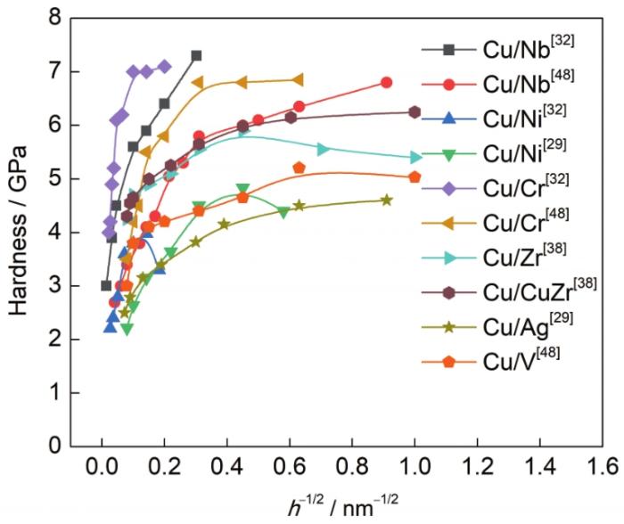
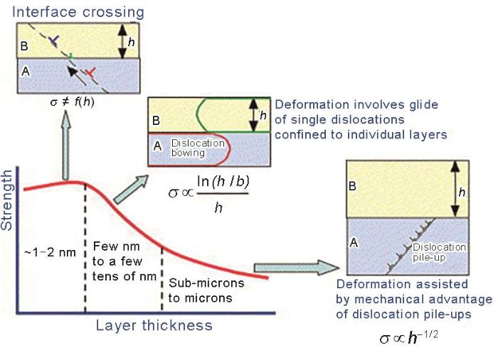
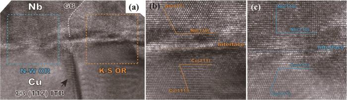
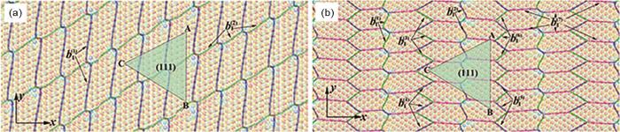
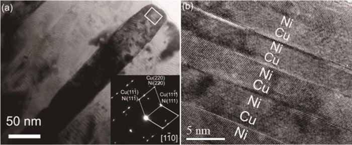
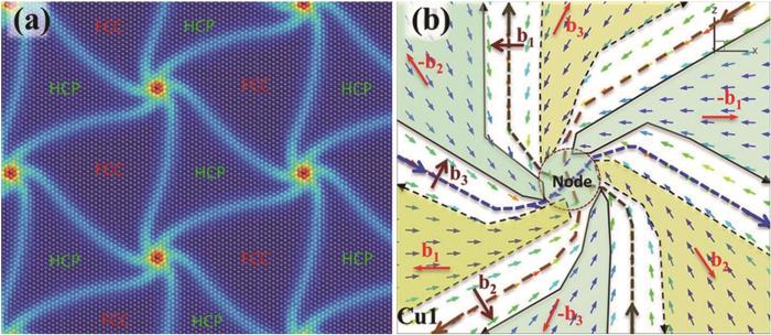
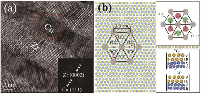
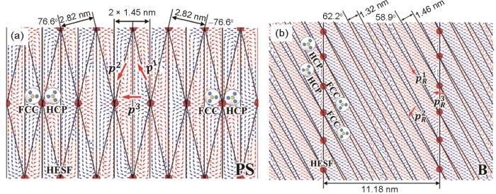


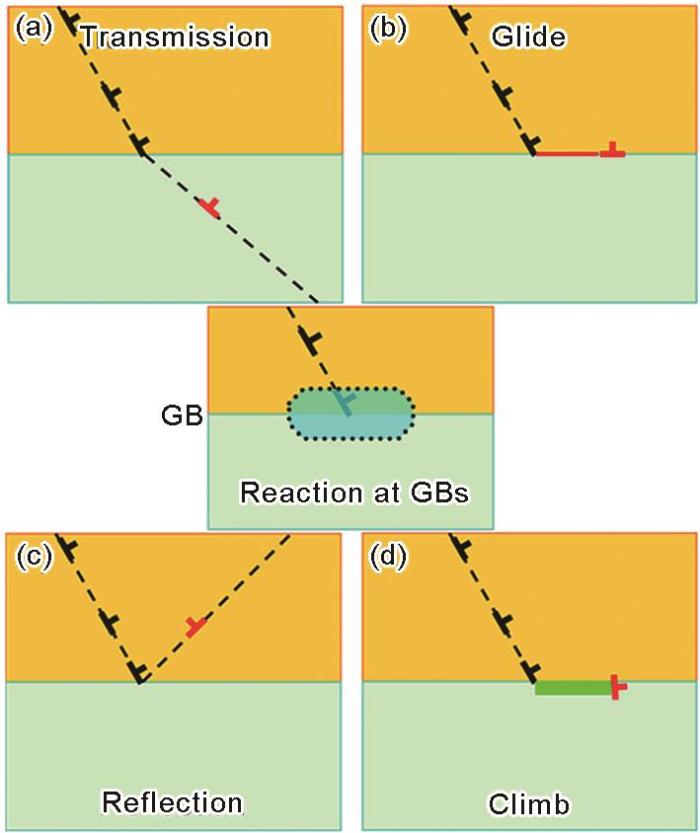
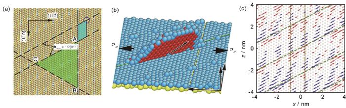
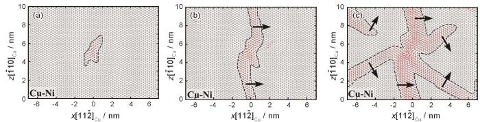
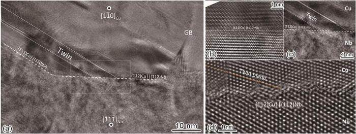
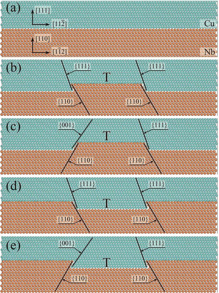

