多场耦合侵蚀下环保Ag/Ti2SnC复合电接触材料的微/纳米力学行为及微结构演变
Micro/Nano-Mechanical Behavior and Microstructure Evolution of Eco-Friendly Ag/Ti2SnC Composite Electrical Contacts Under Multi-Field Coupled Erosion
多场耦合侵蚀下环保Ag/Ti2SnC复合电接触材料的微/纳米力学行为及微结构演变 |
| 丁宽宽, 丁健翔, 张凯歌, 白忠臣, 张培根, 孙正明 |
|
Micro/Nano-Mechanical Behavior and Microstructure Evolution of Eco-Friendly Ag/Ti2SnC Composite Electrical Contacts Under Multi-Field Coupled Erosion |
| DING Kuankuan, DING Jianxiang, ZHANG Kaige, BAI Zhongchen, ZHANG Peigen, SUN Zhengming |
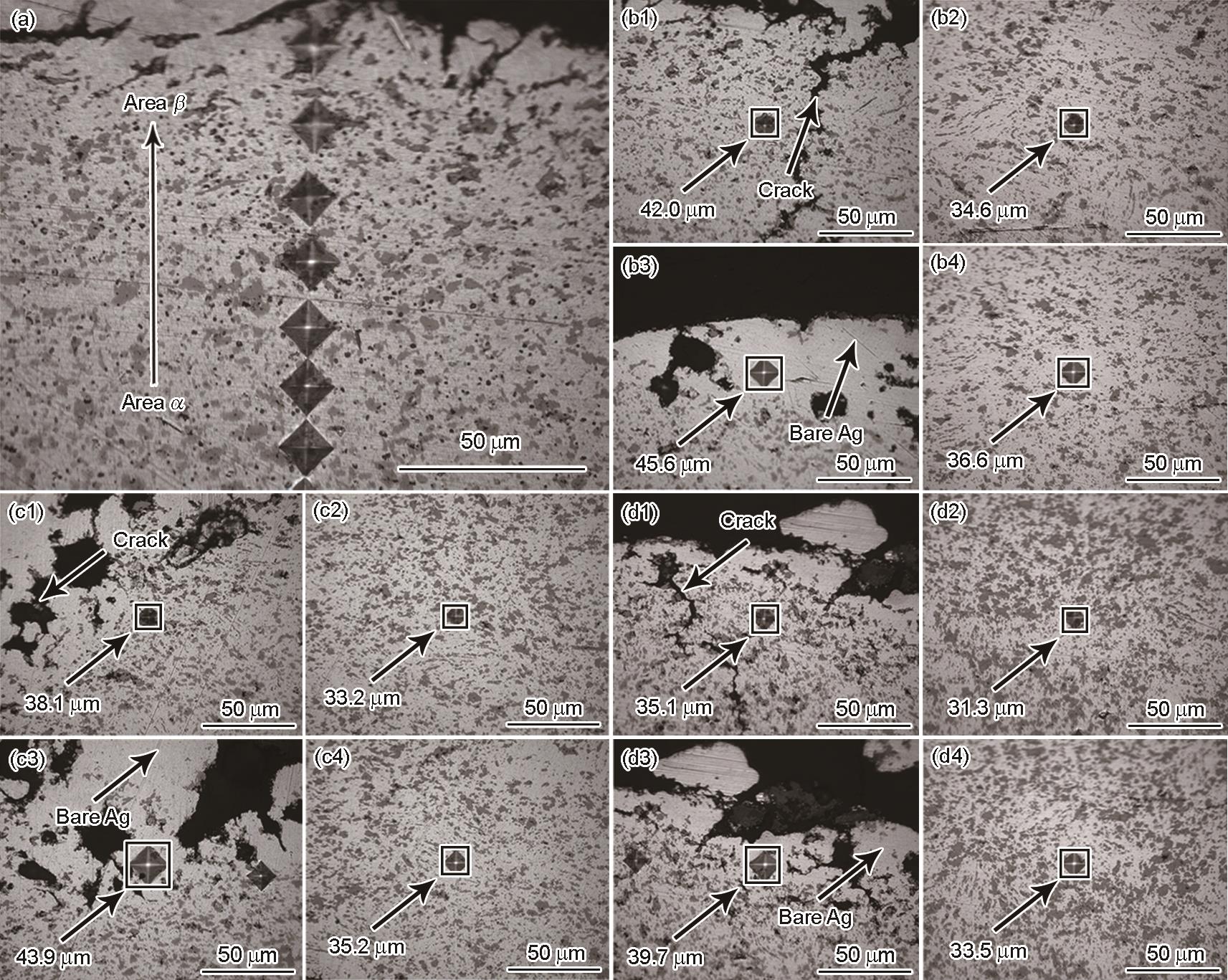
| 图3 Ag/x%Ti2SnC电触头基体内部(区域α)到近电弧侵蚀层(区域β) Vikers硬度压痕OM像 |
| Fig.3 OM images of Vickers micro-hardness indentation position from area α to area β of Ag/x%Ti2SnC contacts with x = 10 (a, b1-b4), x = 12 (c1-c4), and x = 15 (d1-d4) (Numbers show the diagonal diameters of indentations) (b1, b2, c1, c2, d1, d2) indentations on Ti2SnC reinforcing phases of area β (b1-d1) and area α (b2-d2) (b3, b4, c3, c4, d3, d4) indentations on Ag matrix of area β (b3-d3) and area α (b4-d4) |
|
|