p型方钴矿热电材料纳米-介观尺度微结构调控
Nano-Mesoscopic Scale Microstructure Regulation for p-Type Skutterudite Thermoelectric Materials
p型方钴矿热电材料纳米-介观尺度微结构调控 |
| 刘志愿, 王永贵, 赵成玉, 杨婷, 夏爱林 |
|
Nano-Mesoscopic Scale Microstructure Regulation for p-Type Skutterudite Thermoelectric Materials |
| LIU Zhiyuan, WANG Yonggui, ZHAO Chengyu, YANG Ting, XIA Ailin |
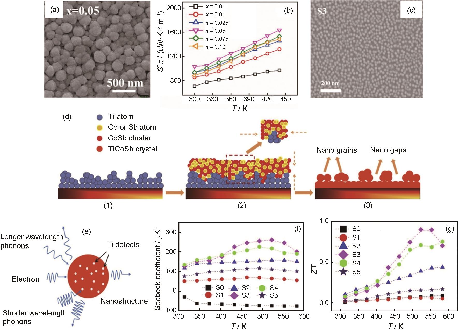
| 图3 Co0.95Fe0.05Sb3薄膜的SEM像[ |
| Fig.3 SEM image of Co0.95Fe0.05Sb3 thin film (a)[ |
|
|