无模板电沉积金属微纳米阵列材料研究进展
A Review on Metal Micro-Nanostructured Array Materials Routed by Template-Free Electrodeposition
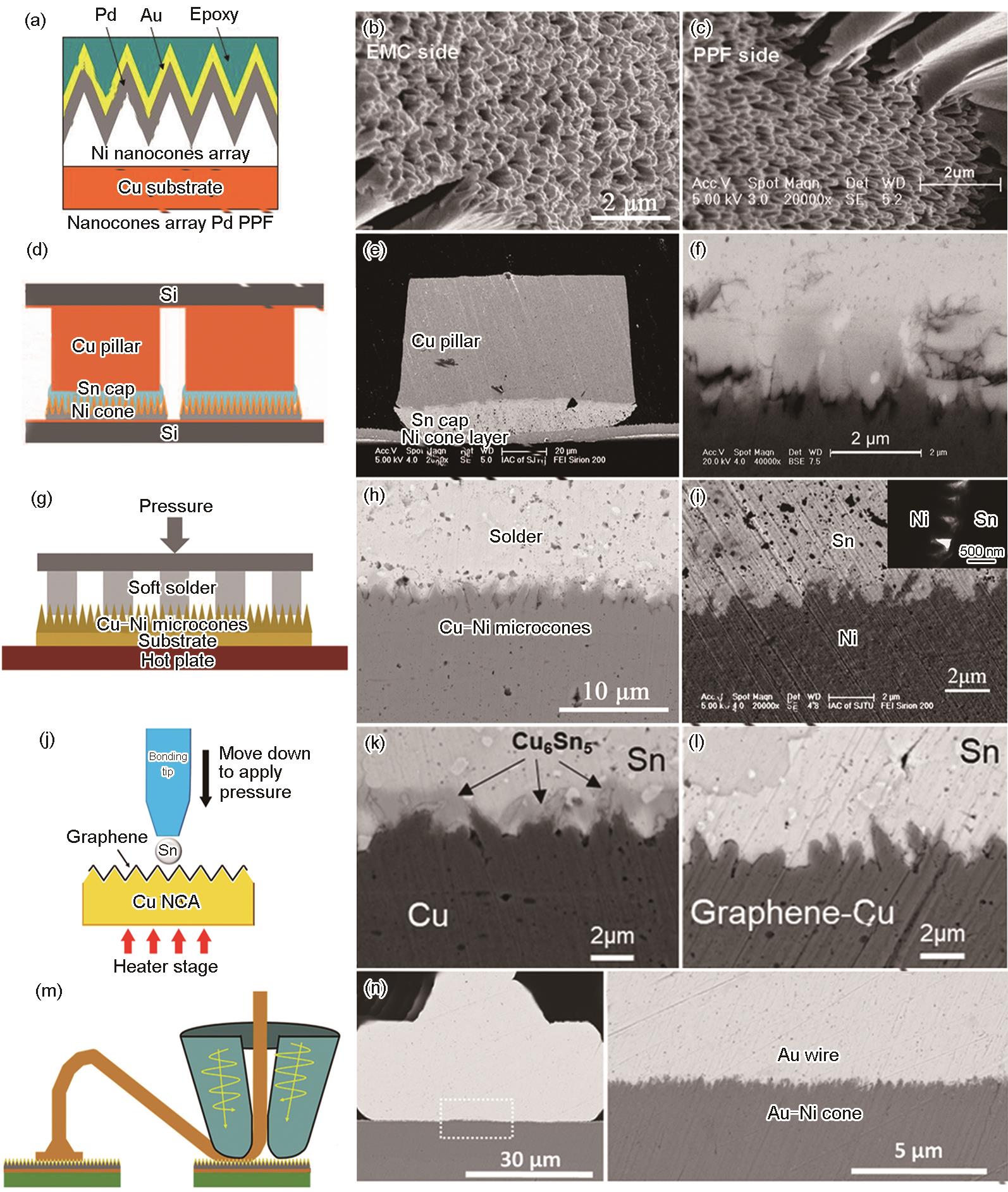
(a) schematic of nano-serrated palladium pre-plated frame (Pd PPF)[
(b, c) SEM images of the interface between nanocones array Pd PPF and molding compound[
(d, g, j, m) schematics of micro-nanocone array bonding and graphene coating micro-nanocone array with Sn-capped Cu bumps (d)[
(e, f, h, i, n) cross-section images of micro-nanocone array bonding with Sn-capped Cu bumps (e, f)[
(k, l) aging behavior comparison between Sn-Cu and Sn-graphene-Cu bonds at 150oC for 96 h[